Organic memory device and method of manufacturing the same

a memory device and organic technology, applied in thermoelectric devices, instruments, nanoinformatics, etc., can solve the problems of increasing reliability, complicating the manufacturing process, and difficult for conventional flash memory devices to have a sufficient cell current device, etc., to achieve uniformity between devices and excellent characteristics

Inactive Publication Date: 2006-06-22
ELECTRONICS & TELECOMM RES INST
View PDF9 Cites 44 Cited by
  • Summary
  • Abstract
  • Description
  • Claims
  • Application Information

AI Technical Summary

Benefits of technology

[0010] The present invention provides an organic memory device which can decrease the size of a device and increase uniformity between cells and the data retention time, and a method of manufacturing the same.
[0022] According to the present invention, a channel exists in a high conductance state or a low conductance state according to an external voltage, and uniformity between devices can be ensured by the use of uniform nano particles, even when highly miniaturized. Accordingly, an organic memory device with excellent characteristics can be provided.

Problems solved by technology

That is, programming or erasing requires a high voltage, which may break down a tunneling oxide layer, thereby decreasing reliability.
However, the consideration of EOT may complicate the manufacturing process.
In addition, it is difficult for conventional flash memory devices to have a sufficient cell current device specific margin when they operate at a low voltage, which is required for low power consumption.
However, based on up-to-date research results, the thermal and chemical stability of polymers or organic materials cannot be guaranteed under memory operating conditions.

Method used


Image

  • Organic memory device and method of manufacturing the same
  • Organic memory device and method of manufacturing the same
  • Organic memory device and method of manufacturing the same

Examples


Embodiment Construction

[0027] The present invention will now be described more fully with reference to the accompanying drawings, in which exemplary embodiments of the invention are shown. The invention may, however, be embodied in many different forms and should not be construed as being limited to the embodiments set forth herein; rather, these embodiments are provided so that this disclosure will be thorough and complete, and will fully convey the concept of the invention to those skilled in the art.

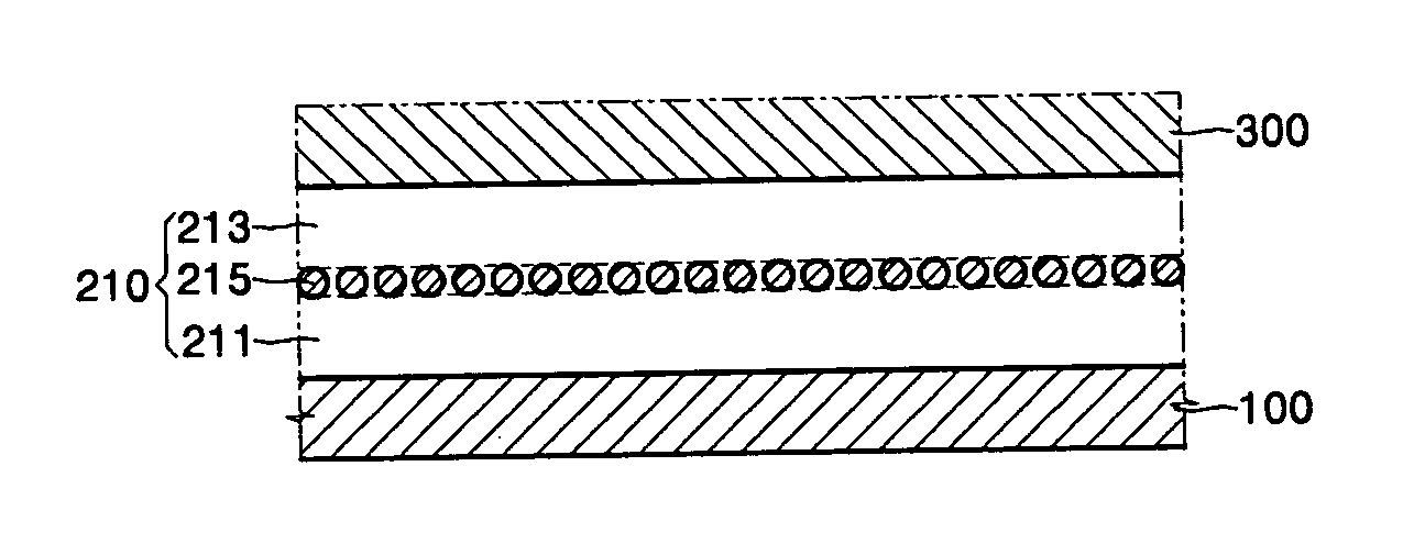
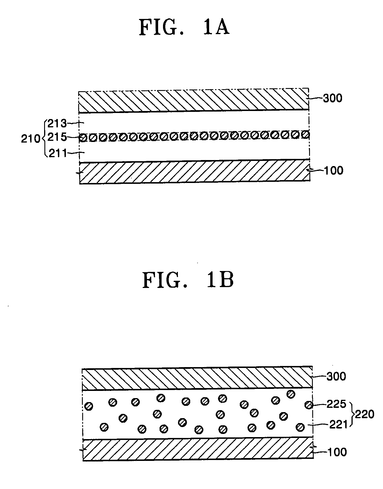
[0028] According to an embodiment of the present invention, an organic memory device has electrical bistability. A conventional organic memory device has a metal electrode / organic material / metal layer / organic material / metal electrode structure, and of these layers, the organic material / metal layer / organic material structure forms an electron channel layer. On the other hand, organic memory devices according to the present invention are characterized by the use of nano particles of a certain size instead of...


PUM


Abstract

An organic memory device and a method of manufacturing the same are disclosed. The organic memory device includes an electron channel layer including an organic layer, in which nano particles of a uniform size are dispersed, interposed between metal electrodes, thus having electrical bistability. The organic memory device uses a change of electrical conductivity which results from a substantial change of the electrical structure of the electron channel layer when a voltage is applied. The organic memory device can be integrated using a simple manufacturing process, and ensures uniformity between devices due to the threshold voltage characteristics, even when highly miniaturized.

Description

CROSS-REFERENCE TO RELATED PATENT APPLICATIONS [0001] This application claims the benefit of Korean Patent Application No. 10-2004-0109296, filed on Dec. 21, 2004, in the Korean Intellectual Property Office, the disclosure of which is incorporated herein in its entirety by reference. BACKGROUND OF THE INVENTION [0002] 1. Field of the Invention [0003] The present invention relates to an electronic device, and more particularly, to a highly integrated organic memory device and a method of manufacturing the same. [0004] 2. Description of the Related Art [0005] Giga-bit DRAMs have been made possible by improvements in semiconductor memory techniques. By the year 2010, it is expected that 100 giga-bit memory devices will be developed. The development of semiconductor memory techniques aids the production of miniaturized semiconductor devices with high speed, large capacity, high integration, low power consumption, and high performance. Ultimately, in a ubiquitous communication environmen...

Claims


Application Information

Patent Timeline
Patent Type & Authority Applications(United States)
IPC IPC(8): H01L29/08H01L23/48H01L29/792H01L29/00H01L29/788
CPCB82Y10/00G11C13/0014G11C13/0016H01L27/285H01L51/0595H10K19/202H10K10/701
Inventor CHOI, SUNG YOOLPARK, CHAN WOOYU, HAN YOUNGPI, UNG HWAN
Owner ELECTRONICS & TELECOMM RES INST
Why Eureka
Try Eureka