Ultra low-loss CMOS compatible silicon waveguides

a technology of cmos and silicon, applied in the direction of optical waveguide light guide, instruments, optics, etc., can solve the problems of high optical loss along the rib waveguide, etchant tends to roughen the exposed sidewall surface, and strip waveguides exhibit relatively high optical loss through their (relatively rough) sidewalls, etc., to achieve low loss and lower loss

Inactive Publication Date: 2006-06-22
CISCO TECH INC +1
View PDF12 Cites 53 Cited by
  • Summary
  • Abstract
  • Description
  • Claims
  • Application Information

AI Technical Summary

Benefits of technology

[0007] The need remaining in the prior art is addressed by the present invention, which relates to the formation of low loss silicon optical waveguides in a silicon-on-insulator (SOI) structure and, more particularly, to the inclusion of a rib / slab of a CMOS-compatible material having a refractive index intermediate that of silicon and silicon dioxide to achieve the desired lower loss.

Problems solved by technology

However, strip waveguides tend to exhibit relatively high optical loss through their (relatively rough) sidewalls, which serve as scattering surfaces for a propagating optical signal.
That is, since an etching process is used to form the sidewalls of the strip, the etchant tends to roughen the exposed sidewall surfaces.
The bulk losses of polysilicon are greater than that of crystalline silicon, resulting in higher optical losses along the rib waveguide.
While this method is somewhat successful in reducing scattering losses, it cannot be used in applications involving “active” waveguide structures, since such a high temperature process will result in unwanted dopant migration within the SOI layer.

Method used


Image

  • Ultra low-loss CMOS compatible silicon waveguides
  • Ultra low-loss CMOS compatible silicon waveguides
  • Ultra low-loss CMOS compatible silicon waveguides

Examples


Embodiment Construction

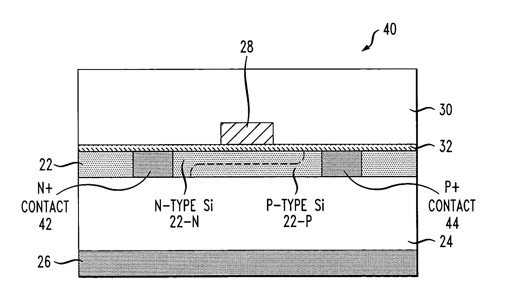
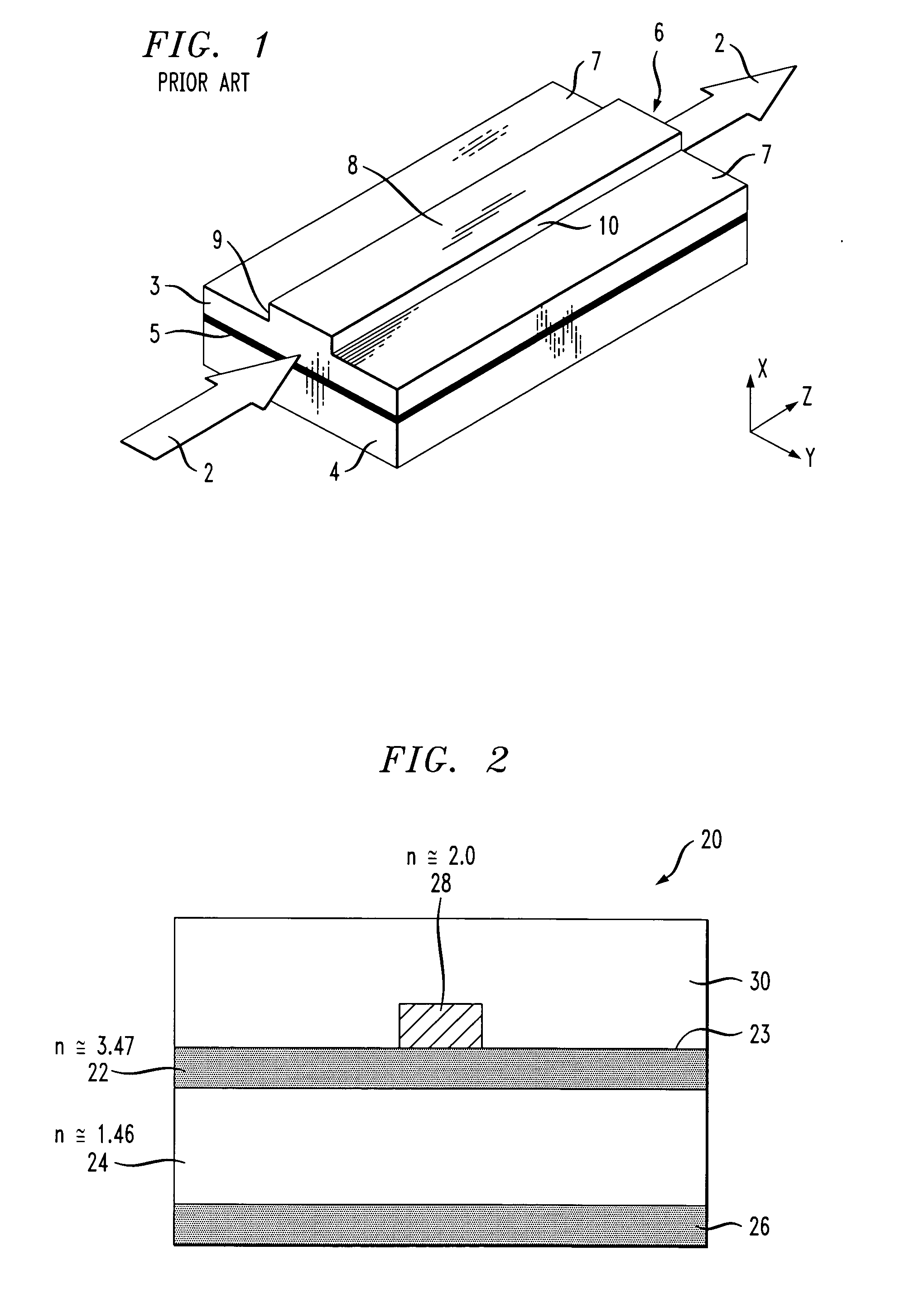
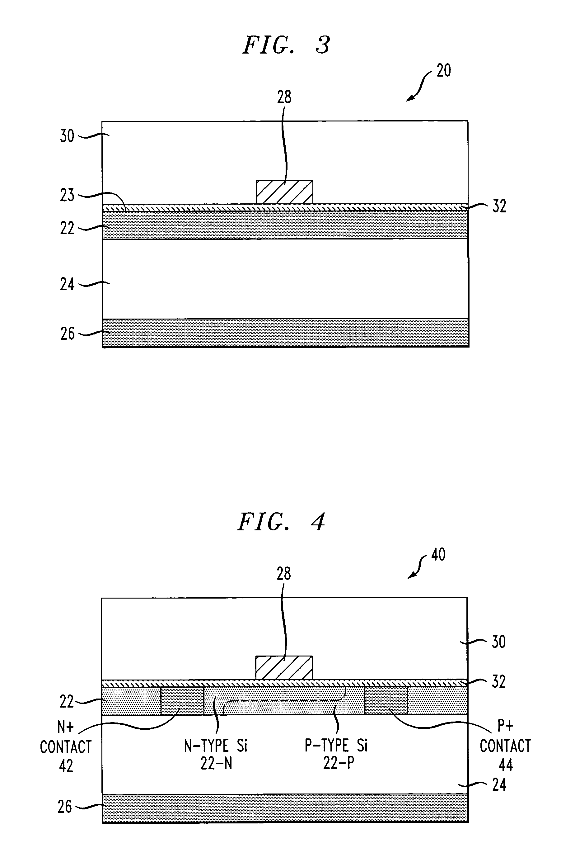
[0023]FIG. 1 illustrates an SOI-based silicon rib waveguide structure 1 as typical in the prior art. The longitudinal z-axis indicates the direction of light propagation, indicated by arrows 2, with the transverse y-direction and x-direction referred to as the “horizontal” and “vertical” directions, respectively. Silicon rib waveguide structure 1 generally consists of a relatively thin single crystal silicon surface layer 3 (generally referred to hereinafter as the “SOI layer”) bonded to a relatively thick silicon substrate 4, with an isolation layer 5 therebetween (thus forming the silicon-on-insulator (SOI) structure). Rib structure 6 is generally fabricated by reactive ion etching (RIE) a pair of parallel trenches 7 in SOI layer 3. Rib structure 6 is defined as having a top surface 8 and opposing sidewalls 9, 10. The optical mode profile O is also shown in FIG. 1. As mentioned above, the use of an etching technique to create sidewalls 9 and 10 results in allowing a significant po...


PUM


Abstract

A low loss optical waveguiding structure for silicon-on-insulator (SOI)-based arrangements utilizes a tri-material configuration including a rib/strip waveguide formed of a material with a refractive index less than silicon, but greater than the refractive index of the underlying insulating material. In one arrangement, silicon nitirde may be used. The index mismatch between the silicon surface layer (the SOI layer) and the rib/strip waveguide results in a majority of the optical energy remaining within the SOI layer, thus reducing scattering losses from the rib/strip structure (while the rib/strip allows for guiding along a desired signal path to be followed). Further, since silicon nitirde is an amorphous material without a grain structure, this will also reduce scattering losses. Advantageously, the use of silicon nitride allows for conventional CMOS fabrication processes to be used in forming both passive and active devices.

Description

CROSS-REFERENCE TO RELATED APPLICATION [0001] The present application claims the benefit of U.S. Provisional Application No. 60 / 638,216, filed Dec. 21, 2004.TECHNICAL FIELD [0002] The present invention relates to the formation of low loss silicon optical waveguides in a silicon-on-insulator (SOI) structure and, more particularly, to the inclusion of a rib / slab of a CMOS-compatible material having a refractive index intermediate that of silicon and silicon dioxide to achieve the desired lower loss. BACKGROUND OF THE INVENTION [0003] The optical waveguides typically formed in SOI-based structures comprise silicon (with a refractive index of approximately 3.47), the silicon formed in a “slab”, “rib” or “strip” geometry on the surface of the SOI substrate. A strip waveguide typically comprises crystalline silicon, where crystalline silicon is known to exhibit less loss that a polysilicon form of the same material. However, strip waveguides tend to exhibit relatively high optical loss th...

Claims


Application Information

Patent Timeline
Patent Type & Authority Applications(United States)
IPC IPC(8): G02B6/10
CPCG02B6/122G02B6/1228G02B2006/12061G02B2006/12097G02F1/025
Inventor PATEL, VIPULKUMARPIEDE, DAVIDGHIRON, MARGARETGOTHOSKAR, PRAKASH
Owner CISCO TECH INC
Why Eureka
Try Eureka