Nanoscale electronic detection system and methods for their manufacture

a technology of electronic detection and nano-scale, applied in the field of detection devices, can solve the problems that the dna plating process is often implemented in the same technique for hours, and achieve the effect of extraordinary signal-to-noise ratio and rapid electroplating

Inactive Publication Date: 2006-06-22
NANOGEN INC
View PDF0 Cites 17 Cited by
  • Summary
  • Abstract
  • Description
  • Claims
  • Application Information

AI Technical Summary

Benefits of technology

[0016] A new, extremely sensitive, and rapid electronic detection method for direct detection of hybridized genomic targets to specific probes on the microarray is proposed. The method consists of fast electronic accumulation of the DNA target on a particular electrode site at the micro-electrode array, sequential electronic hybridization of oligonucleotide labeled metallic (nano)particles on the target DNA and monitoring the electrochemical AC impedance changes at the electrode site. The method is enhanced by electroplating over the DNA target which serves as the metallization template and over the particles which provide seeds for rapid electroplating. The AC impedance changes are monitored during the electroplating over the DNA target and between the array electrodes sites. The signal in the absence and presence of the target DNA is a difference between “no connection” and a “short” between the array electrodes. This assures an extraordinary signal-to-noise ratio. The method offers unprecedented sensitivity, theoretically approaching single or only a few DNA molecules attached to the electrode site. Rapid electronic addressing of the DNA target and labeled nanoparticles to the microarray assures that the detection at these levels of sensitivity will be achieved within only a few minutes.

Problems solved by technology

These techniques often take hours to implement the DNA plating process and are not site specific.

Method used


Image

  • Nanoscale electronic detection system and methods for their manufacture
  • Nanoscale electronic detection system and methods for their manufacture
  • Nanoscale electronic detection system and methods for their manufacture

Examples


Embodiment Construction

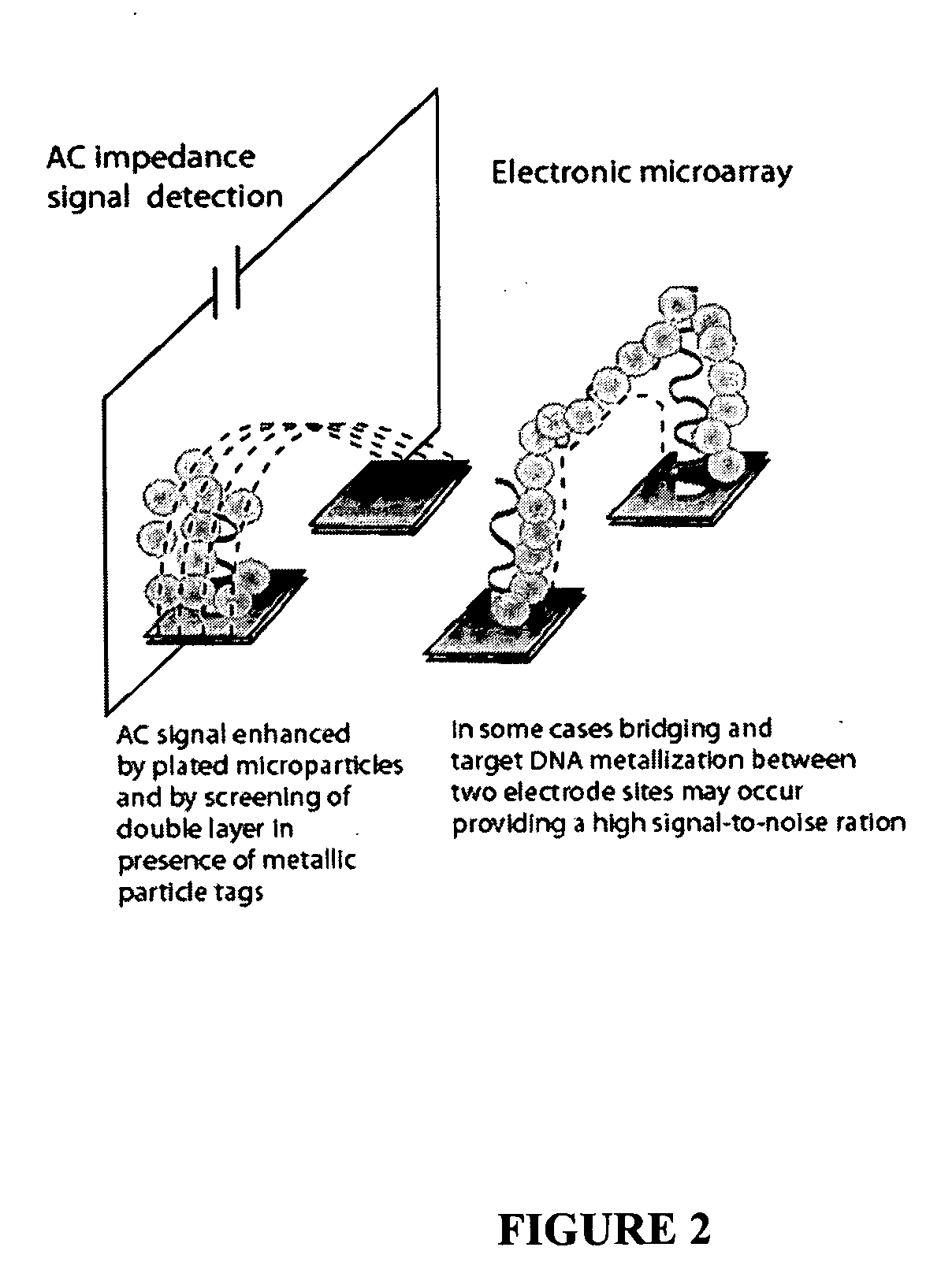
[0029] AC Impedance System for Detection of DNA-Templated Electroplating

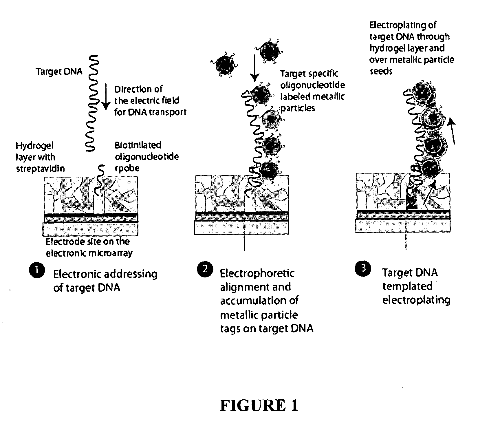
[0030]FIG. 1 shows a schematic diagram of the proposed electronic detection system for specific and highly sensitive detection of DNA targets. The detection consists of the following steps.

[0031] Electronic addressing of the target DNA occurs first. This step occurs in accordance to Nanogen's developed technology and implies accumulation of low concentration of DNA targets at an electrode array site from solution by electrophoresis. The electronic microarray is covered by a hydrogel permeation layer (ca 7-10 micron thick) containing streptavidin molecules. The proposed system assumes the use of pre-loaded biotinilated probes complementary to a particular gene region of interest on the target DNA. The target DNA can be very rapidly, within less than one minute, accumulated from the solution and electronically hybridized at a particular array site, providing a localization of the detection process.

[0032] Once t...


PUM

PropertyMeasurementUnit
weightaaaaaaaaaa
diameteraaaaaaaaaa
thickaaaaaaaaaa

Abstract

A new, extremely sensitive, and rapid electronic detection method for direct detection of hybridized genomic targets to specific probes on the microarray is proposed. The method consists of fast electronic accumulation of the DNA target on a particular electrode site at the micro-electrode array, sequential electronic hybridization of oligonucleotide labeled metallic (nano)particles on the target DNA and monitoring the electrochemical AC impedance changes at the electrode site. The method is enhanced by electroplating over the DNA target which serves as the metallization template and over the particles which provide seeds for rapid electroplating. The AC impedance changes are monitored during the electroplating over the DNA target and between the array electrodes sites. The signal in the absence and presence of the target DNA is a difference between “no connection” and a “short” between the array electrodes

Description

RELATED APPLICATIONS [0001] This application claims priority to U.S. Provisional Application Ser. No. 60 / 575,445, filed May 28, 2004, entitled “Nanoscale Electronic Detection System”, and is incorporated herein by reference as if fully set forth herein.FIELD OF THE INVENTION [0002] This invention relates to microscale and nanoscale electronic systems and methods for their manufacture. More particularly, the apparatus and methods relate to detectors, especially single sequence detection systems. BACKGROUND OF THE INVENTION [0003] Sequencing of the Human Genome induced a new knowledge in understanding the correlations between the DNA structure, gene functions, efficiency of targeted therapeutics as well as occurrence and development of a variety of genetic and infectious diseases. Molecular diagnostics based on DNA revealed mechanisms and advancement of numerous dangerous diseases including cancer, HIV, cystic fibrosis, heart and lung diseases, emerging infectious diseases, to name a ...

Claims


Application Information

Patent Timeline
Patent Type & Authority Applications(United States)
IPC IPC(8): C12Q1/68B01L3/00B01L9/00
CPCB01L3/5027B01L9/527C12Q1/6825C12Q2563/155C12Q2563/137C12Q2565/607C12Q2565/501G01N27/3278
Inventor HODKO, DALIBORSMOLKO, DANIELDUFFY, STUART F.
Owner NANOGEN INC
Why Eureka
Try Eureka