Process for forming MEMS

a technology of forming process and machining method, which is applied in the manufacture of microstructural devices, microstructures, electrical devices, etc., can solve the problems of not being able to achieve the effect of extending the structural stability of the machining method, unable to generally be done through both the photoresist and the primary metal, and not being able to remove the photoresist first before the machining of the primary metal

a technology of forming process and machining method, which is applied in the manufacture of microstructural devices, microstructures, electrical devices, etc., can solve the problems of not being able to achieve the effect of extending the structural stability of the machining method, unable to generally be done through both the photoresist and the primary metal, and not being able to remove the photoresist first before the machining of the primary metal

US20060134819A1Active Publication Date: 2006-06-22FORMFACTOR INC

Image

  • Process for forming MEMS
  • Process for forming MEMS
  • Process for forming MEMS

Examples


Embodiment Construction

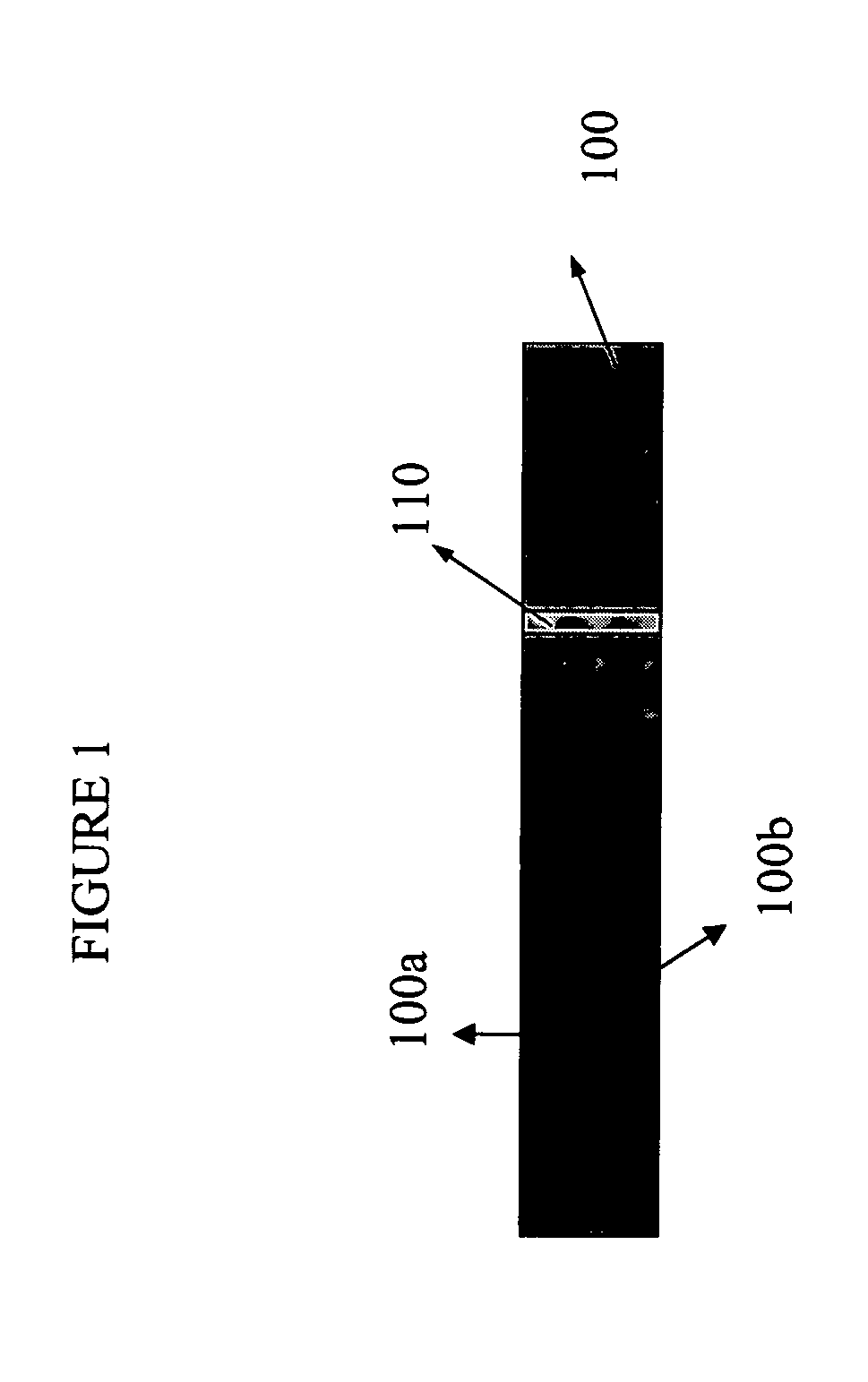
[0013]FIG. 1 shows a starting material on which to build the microstructure. The substrate 100 may be any type of substrate, including semiconductors such as silicon, germanium and gallium arsenide, ceramics such as alumina, aluminum, nitride low temperature cofired ceramics (LTCC) and high temperature cofired ceramics (HTCC), metals or glasses. In an embodiment of the present invention, microstructures such as springs used in testing semiconductor devices may be built on the substrate 100. In that case, the substrate 100 may be a Low Temperature Co-fired Ceramic (LTCC) substrate with built in vias 110 such that electricity may be conducted from one face 100a of the substrate 100 to the other face 100b of the substrate 100 by way of the vias 110. In an embodiment of the present invention, the vias 110 are made from gold, but any other conductor such as copper or platinum may be used. The ceramic may also contain electrical redistribution conductors, making it an electrical “space tr...


PUM

PropertyMeasurementUnit
areaaaaaaaaaaa
heightaaaaaaaaaa
mechanical stabilityaaaaaaaaaa

Abstract

The present invention relates to a process for forming microstructures on a substrate. A plating surface is applied to a substrate. A first layer of photoresist is applied on top of the plating base. The first layer of photoresist is exposed to radiation in a pattern to render the first layer of photoresist dissolvable in a first pattern. The dissolvable photoresist is removed and a first layer of primary metal is electroplated in the area where the first layer of photoresist was removed. The remainder of the photoresist is then removed and a second layer of photoresist is then applied over the plating base and first layer of primary metal. The second layer of photoresist is then exposed to a second pattern of radiation to render the photoresist dissolvable and the dissolvable photoresist is removed. The second pattern is an area that surrounds the primary structure, but it does not entail the entire substrate. Rather it is an island surrounding the primary metal. The exposed surface of the secondary metal is then machined down to a desired height of the primary metal. The secondary metal is then etched away.

Description

BACKGROUND [0001] The formation of micromechanical structures using photolithography and sacrificial layers is known in the art. The present invention is an improvement to the technology disclosed in U.S. Pat. No. 5,190,637 to Gluckel, titled “Formation of Microstructures by Multiple Level Deep X-ray Lithography with Sacrificial Metal Layers,”(“the '637 patent”), which is incorporated herein by reference. In the '637 patent, microstructures are built in several steps. First a layer of photoresist capable of exposure by Radiation is applied to a plating base. The photoresist is then exposed to Radiation using a mask. The mask allows the Radiation to only “expose” a certain defined area of the photoresist. Subsequent developing removes photoresist selective to the exposure creating a cavity that replicates the plan of the exposure mask. The cavity formed in the photoresist is then filled by a primary metal that is electroplated on to an exposed plating base. The remaining photoresist ...

Claims


Application Information

Patent Timeline
22 Jun 2006
Publication
US20060134819A1
IPC
H01L21/00; H01L21/302
CPC
B81C1/00666; B81C2201/0109; B81C2201/0197
Inventors
TANG, WEILONG; HSU, TSENG-YANG