Light-scattering film and optical device using the same

Inactive Publication Date: 2006-06-29
MITSUBISHI HEAVY IND LTD
View PDF8 Cites 32 Cited by
  • Summary
  • Abstract
  • Description
  • Claims
  • Application Information

AI Technical Summary

Benefits of technology

[0013] Another object of the present invention is to provide a new technique f

Problems solved by technology

However, undesired effect may also be generated if the concavities and convexities are provided to a conductive material for the purpose of scattering the light.
For example, in the photoelectric conversion device, the usage of the transparent electrode formed in the textured form, as the electrode on the side of the substrate, induces defects to a semiconductor thin film formed thereon.
This indicates that the improvement of the conversion efficiency of the photoelectric conversion device is limited, in the technique using the transparent electrode formed in the textured form

Method used


Image

  • Light-scattering film and optical device using the same
  • Light-scattering film and optical device using the same
  • Light-scattering film and optical device using the same

Examples


first embodiment

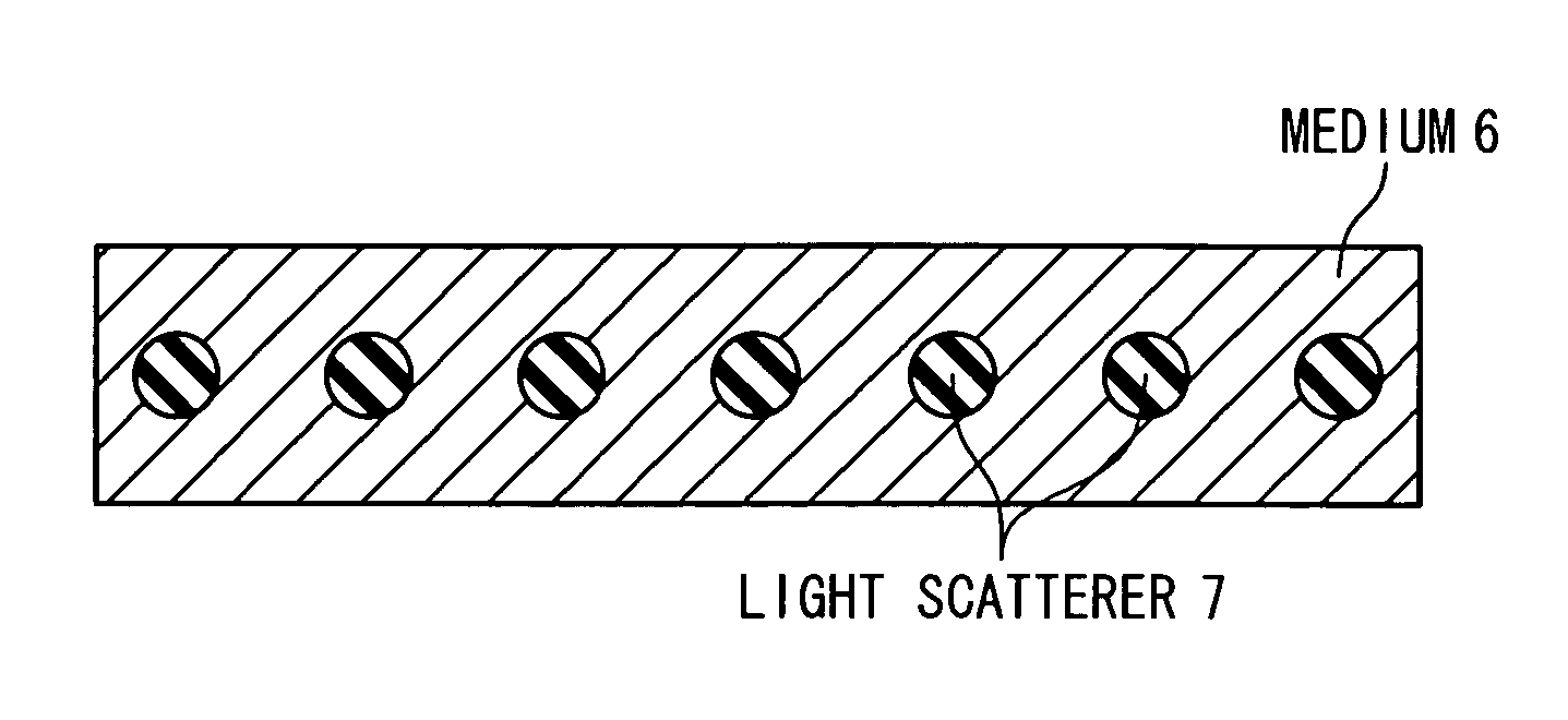
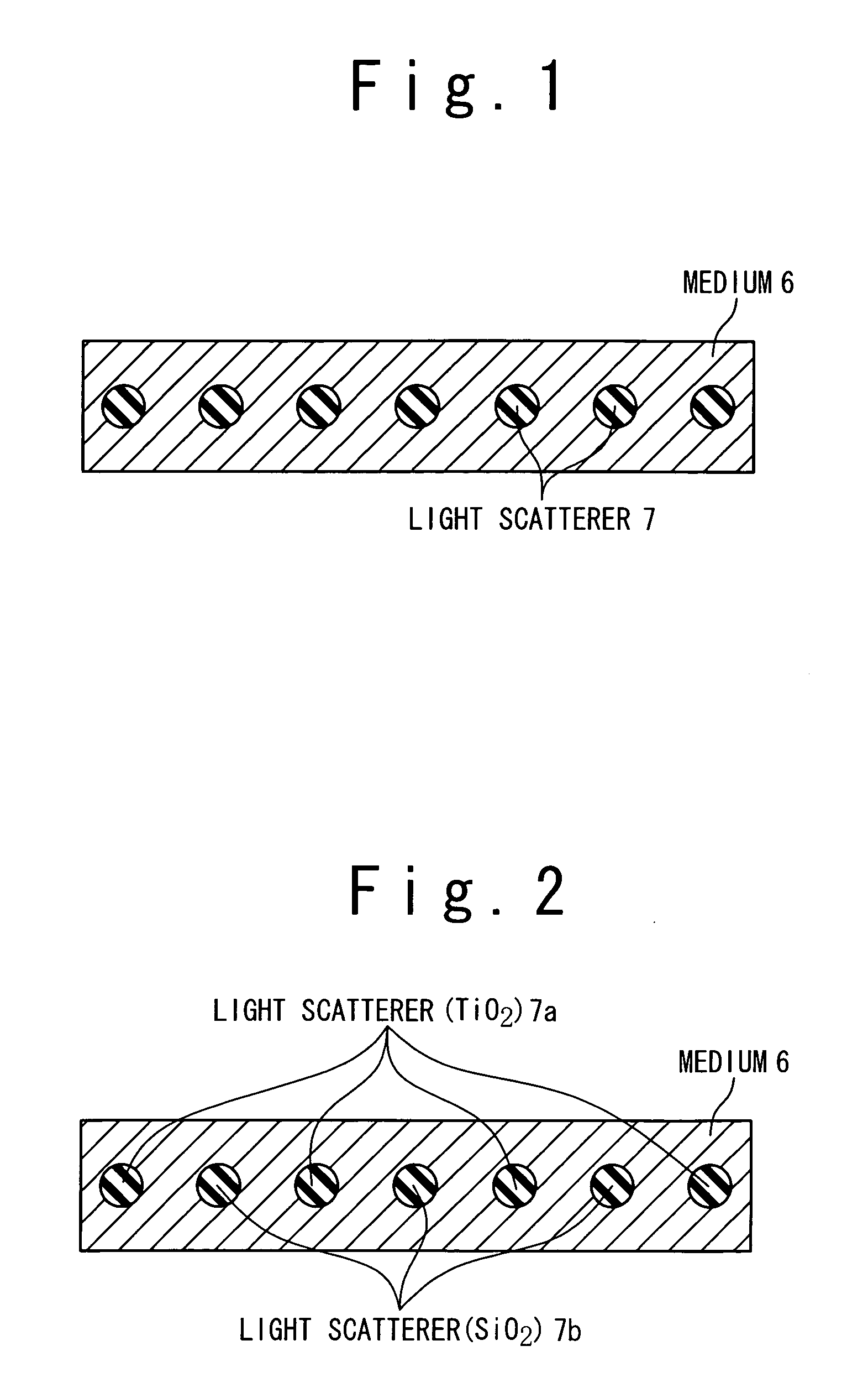
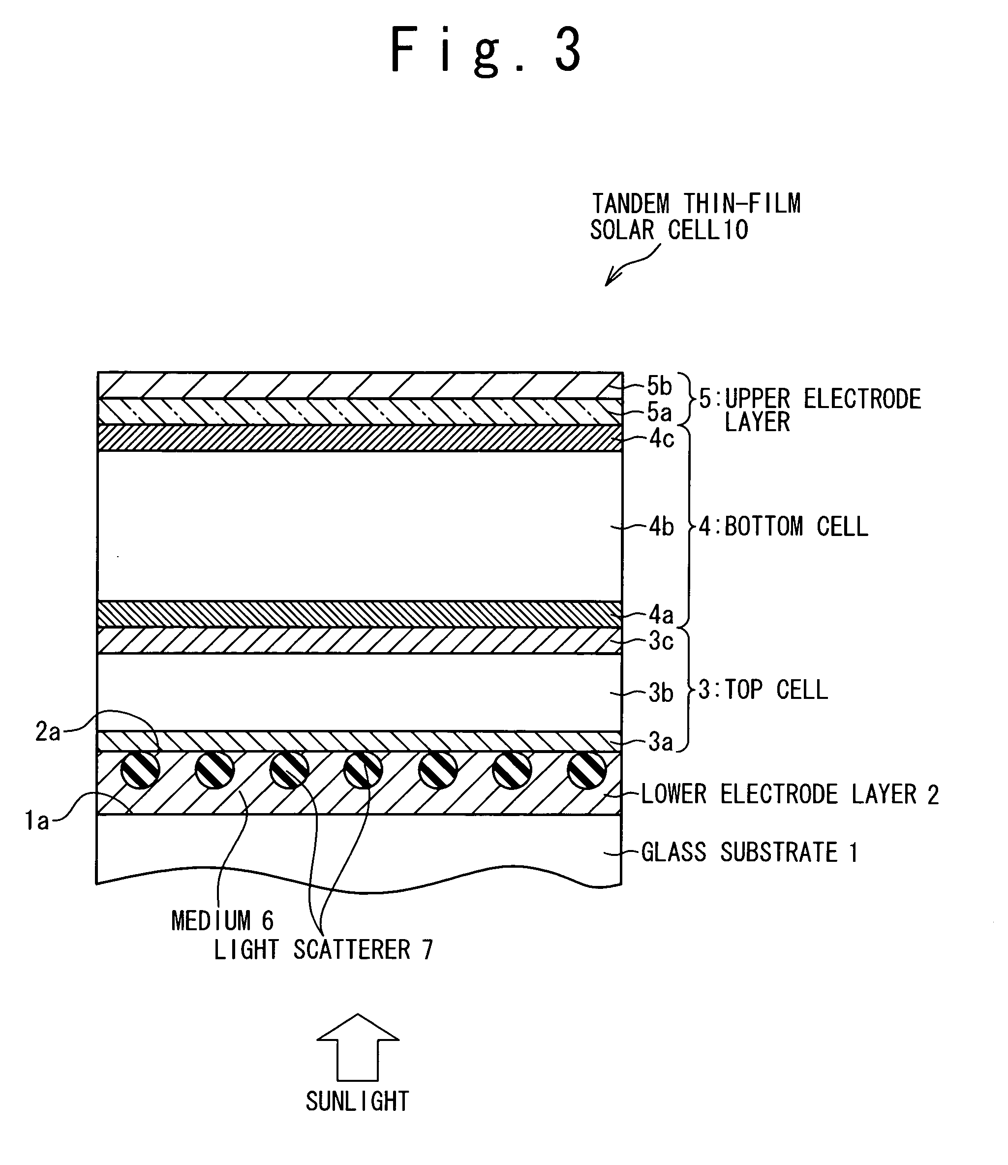
[0050] In the first embodiment, a light-scattering film of the present invention is used as a transparent electrode of a photoelectric conversion device. In the embodiment, a tandem thin-film solar cell 10 is configured with a glass substrate 1, and is further configured with a lower electrode layer 2, a top cell 3, a bottom cell 4, and an upper electrode layer 5, which are formed in order on a principal surface 1a of the glass substrate 1, as shown in FIG. 3. The top cell 3 includes a p-type amorphous silicon layer 3a, an i-type amorphous silicon layer 3b, and an n-type amorphous silicon layer 3c, which are formed in order on the lower electrode layer 2. The bottom cell 4 includes a p-type microcrystalline silicon layer 4a, an i-type microcrystalline silicon layer 4b, and an n-type microcrystalline silicon layer 4c, which are formed in order on the top cell 3. The upper electrode layer 5 includes a ZnO layer 5a formed on the bottom cell 4, and an Ag layer 5b formed on the ZnO layer...

second embodiment

[0076] In the second embodiment, a light-scattering layer of the present invention is used as an electrode of a reflective liquid crystal display device, as shown in FIG. 11. In the reflective liquid crystal display device, it is required that outside light incident to the reflective liquid crystal display device is reflected, and further, scattered. The light-scattering film of the present invention is used as the electrode for applying a desired voltage to a liquid crystal, and as a light-scattering means to scatter the light.

[0077] More specifically, the reflective liquid crystal display device of the second embodiment is provided with a transparent substrate 31, an opposed substrate 32, a transparent electrode 33, an opposed electrode 34, and a polarizing film 35. The transparent substrate 31 and the opposed substrate 32 are supported to face to each other by a spacer 39, and a liquid crystal 36 is filled between the transparent substrate 31 and the opposed substrate 32. The tr...

third embodiment

[0081] In the third embodiment, a light-scatteinring layer of the present invention is used as an electrode of an organic EL (electroluminescence) element, as shown in FIG. 12. In the organic EL element, scattering of light generated by the organic EL element is useful in some cases. For example, when the organic EL element is used for a display device, the scattering of the generated light is useful for improving visibility of the display device. In this embodiment, the light-scattering layer of the present invention supplies an electric current to a light-emitting layer, and is further used to scatter the light.

[0082] More specifically, the organic EL element of the third embodiment is provided with a transparent substrate 41, a positive pole 42, a positive-hole transport layer 43, a light-emitting layer 44, an electron transport layer 45, and a negative pole 46. In the organic EL element, the positive holes are injected from the positive pole 42 to the light-emitting layer 44 th...


PUM


Abstract

A light scattering film having the structure which guides electrical signal to a desired position and scatters incident light and the surface of which is substantially flat, and a photoelectric device using the same. The light scattering film includes a medium made of transparent conductive material and a light scatterer embedded in the medium. The light scattering film realizes conductivity and the light-scattering characteristic by single component. It is not necessary to make the texture of a surface with concavity and convexity deliberately to achieve the light-scattering characteristic. Desirably, the surface is substantially flat. When a semiconductor layer is formed on the surface, the defects are suppressed because of the flatness of the surface. The photoelectric device having the light scattering film and the semiconductor device on the surface of the film can achieve high photoelectric conversion efficiency.

Description

BACKGROUND OF THE INVENTION [0001] 1. Field of the Invention [0002] The present invention relates to a light-scattering film and an optical device using the same. [0003] 2. Description of the Related Art [0004] One of the devices sustaining the modern life is an optical device that realizes desired functions by utilizing the mutual conversion between electricity and light. A photoelectric conversion device (for example, a solar cell), a light-emitting device (for example, an electroluminescent element exemplified by a light-emitting diode and an OLED (organic light emitting diode)), and a liquid crystal element (for example, a liquid crystal display panel), are typical optical devices. Such optical devices are indispensable to the modern daily life. [0005] An optical device includes a conductive structure member for guiding an electrical signal (for example, an electric current and a voltage) to a desired position, and a structure member for scattering light. For example, Japanese L...

Claims


Application Information

Patent Timeline
IPC IPC(8): H01L31/00G02B5/02G02F1/1335G02F1/1343G09F9/30H01L31/04H01L51/50H05B33/28
CPCG02F1/133504G02F2202/16H01L31/02168H01L31/0547H01L31/0232H01L2933/0091Y02E10/52H01L31/022466Y02E10/548H01L31/076H01L31/054H01L31/056
Inventor KOBAYASHI, YASUYUKISAKAI, SATOSHISATAKE, KOJI
Owner MITSUBISHI HEAVY IND LTD
Why Eureka
Try Eureka