Manipulation of conductive and magnetic phases in an electron trapping semiconducting

a technology of semiconducting and magnetic phase, applied in the field of semiconducting strip array, can solve the problems of complex simulation of hubbard and t-j models, difficult miniaturization of the setup, and complete disagreement and confusion in the physics community regarding the precise mechanism and the exact model parameters

Inactive Publication Date: 2006-06-29
UNIV OF UTAH RES FOUND
View PDF6 Cites 12 Cited by
  • Summary
  • Abstract
  • Description
  • Claims
  • Application Information

AI Technical Summary

Benefits of technology

[0012] The present invention has been developed in response to the above and other needs in the art. Briefly summarized, embodiments of the present invention are directed to a semiconductor strip array that can be configured so as to exhibit a number of distinct physical phases, each of which has its own distinct electrical and/or magnetic characteristics. The strip array can be incorporated into MOSFET geometry and utilized in amplifier and memory cell applications. Significantly, the strip array can exhibit superconductive characteristics under relatively high temperature conditions. In one embodiment, the strip array comprises a substrate and a plurality of strips deposited on the substrate in an intersecting pattern to define the strip array. The intersecting strip array defines primary electron trapping sites at the strip intersections and secondary electron trapping sites within the individual strips, half-way between intersections. The strip array is further configured to exhibit distinct electrical and/or magnetic properties, strictly as a function of the concentration of electrons that are introduced into the primary and secondary electron trapping sites respectively, regardless of the means by which these electrons are introduced. This concentration of extraneous electrons can be varied continuously by external means, from zero to several electrons per cell. As the electron concentration is varied, a number of distinct insulating conductive, semiconductive, and superconductive states can be realized.
[0013] In another aspect of the present invention, a method for changing the electromagnetic properties of a semiconductor strip array is disclosed. The strip array includes a plurality of intersecting strips of semiconductor material deposited on a substrate. The intersections of the strips define primary electron trapping sites, and the portions of the strips between the strip intersections define secondary electron trapping sites. The method for selectively changing the electronic properties of the strip array includes the introduction (by whatever means) of a quantity of electrons into the array, e.g. so that a portion of the primary electron trapping sites—say 10% to 70% of them—are occupied by electrons. This will cause th...

Problems solved by technology

However, there is complete disagreement and confusion in the physics community regarding the precise mechanism and the exact model parameters that apply.
Computer simulations of the Hubbard and t-J models have failed to be definitive, owing to the difficulty of solving the many-fermion problem on a sufficiently large lattice—even approximately.
But this set-up is difficult to miniaturize, as the power expended in electrical currents can quickly exceed the ability of the material to dissipate and causes meltdown when circuit elements are den...

Method used


Image

  • Manipulation of conductive and magnetic phases in an electron trapping semiconducting
  • Manipulation of conductive and magnetic phases in an electron trapping semiconducting
  • Manipulation of conductive and magnetic phases in an electron trapping semiconducting

Examples


Embodiment Construction

[0039] Reference will now be made to figures wherein like structures will be provided with like reference designations. It is understood that the drawings are diagrammatic and schematic representations of exemplary embodiments of the invention, and are not limiting of the present invention nor are they necessarily drawn to scale.

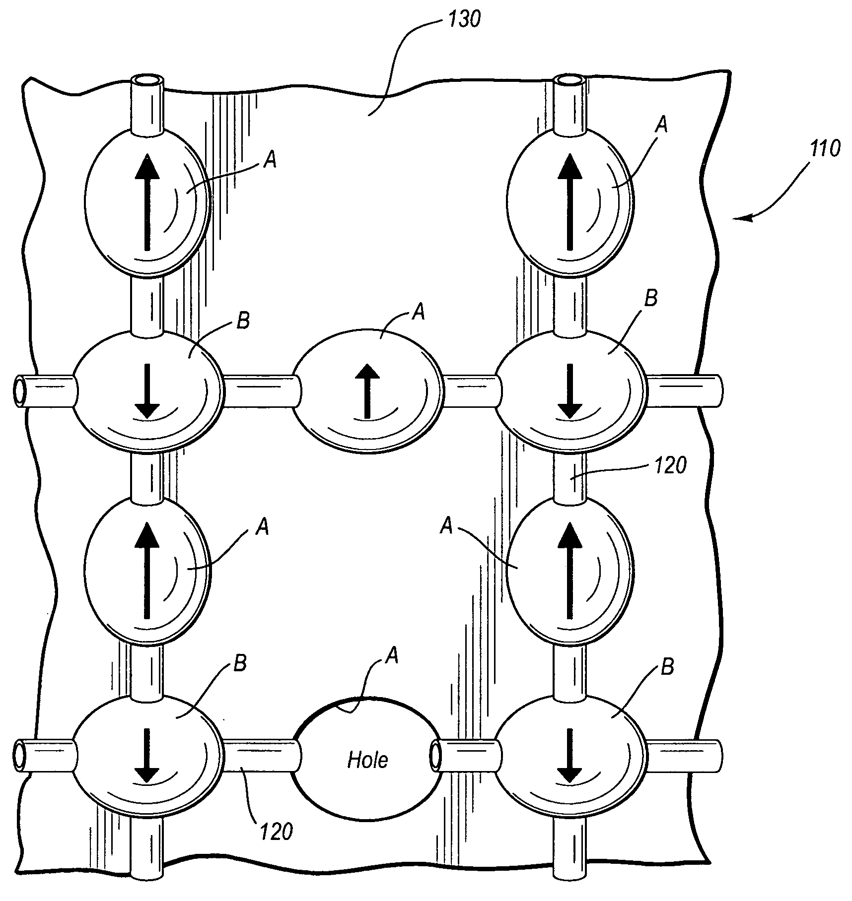
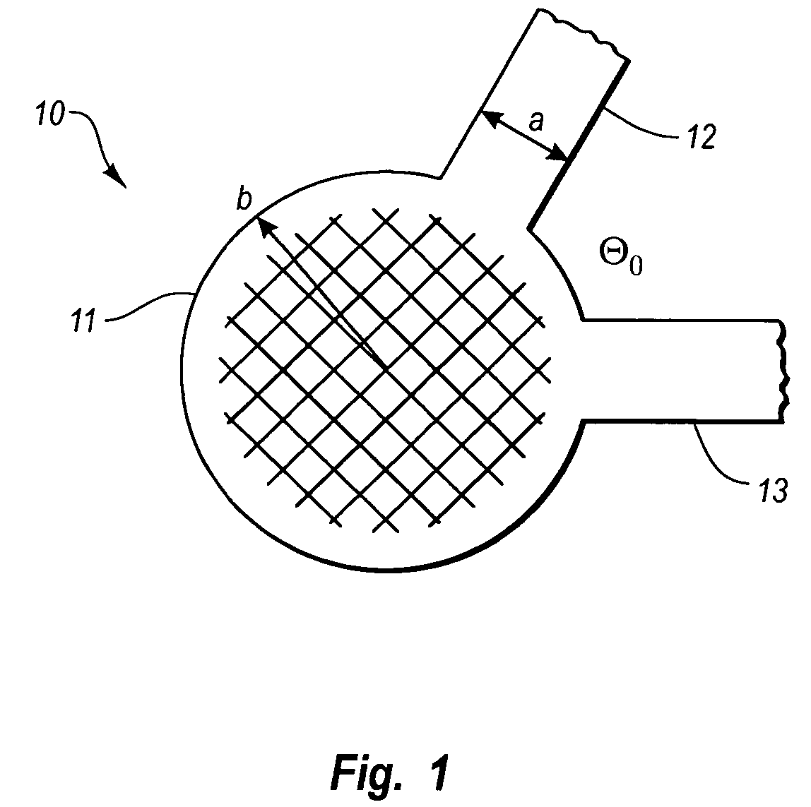
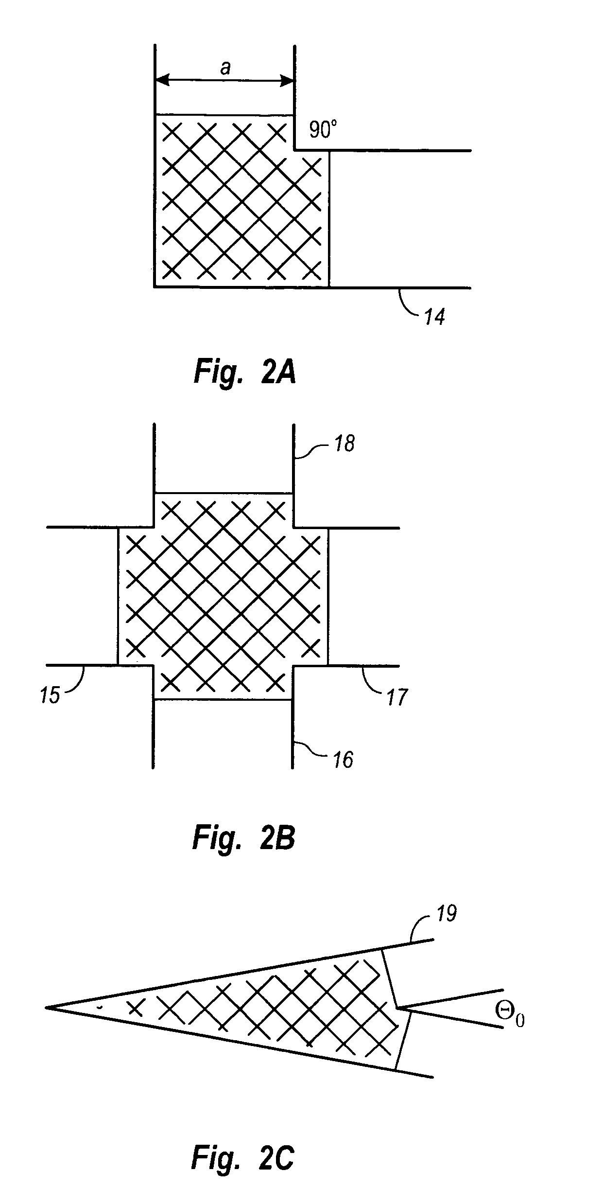
[0040] The present invention uses a recently discovered property of particles in narrow spaces as the building block in a new concept for the creation of synthetic structures to make artificial atoms and molecules. The terms “particle” or “particles” used herein refers to subatomic particles such as electrons, photons, excitons, phonons, and the like.

[0041] The present invention applies techniques for particle localization by geometrical nanostructures that allow for the production of artificial atoms, and from them, small or large molecules and arrays suitable for use in electronic devices. While the present invention uses procedures based on currently av...


PUM


Abstract

A semiconductor strip array that can be configured to exhibit distinct electrical and/or magnetic phase characteristics according to the many-body effects phenomenon in electron gases is disclosed. The strip array can be incorporated into a MOSFET architecture and utilized in amplifier and memory cell applications. Significantly, the strip array can exhibit superconductive characteristics under relatively high temperature conditions. In one embodiment, the strip array comprises a grounded substrate, a plurality of strips deposited on the substrate in an intersecting pattern to define the strip array, an insulating layer atop the array, a source, and a drain. The intersecting strip array defines primary electron trapping sites at the strip intersections and secondary electron trapping sites on the strips between the intersections. The strip array is further configured to exhibit distinct electrical and/or magnetic properties according to a selective concentration of electrons injected into the primary and secondary electron trapping sites.

Description

RELATED APPLICATIONS [0001] This application is a continuation-in-part of the following U.S patent applications: application Ser. No. 10 / 737,178, filed Dec. 16, 2003, and entitled “Signal Amplification Using Architectures of Nanodots and Connecting Channels,” which claims the benefit of provisional Application No. 60 / 433,738, filed Dec. 16, 2002; and application Ser. No. 11 / 122,948, filed May 5, 2005, and entitled “Artificial Ferromagnetism in Semiconducting Arrays,” which claims the benefit of provisional Application No. 60 / 568,381, filed May 5, 2004. Each of these applications is incorporated herein by reference in its entirety.BACKGROUND [0002] 1. Technology Field [0003] The present invention generally relates to semiconductive nanostructures. In particular, the present invention relates to a semiconductor strip array that is configured to be modified so as to exhibit varying electrical and magnetic properties based on electron concentration. [0004] 2. The Related Technology [000...

Claims


Application Information

Patent Timeline
IPC IPC(8): H01L29/06H01L27/14H01L31/109
CPCH01L39/146H10N60/207
Inventor MATTIS, DANIEL C.
Owner UNIV OF UTAH RES FOUND
Why Eureka
Try Eureka