Atomic layer deposition using metal amidinates

a technology of amidinate and atomic layer, which is applied in the direction of group 5/15 element organic compounds, organic chemistry, coatings, etc., can solve the problems of self-limiting ald reactions, no data published to demonstrate that the proposed surface reaction is actually self-limiting, and copper from this ald process only grows on pre-existing platinum surfaces. , to achieve the effect of high electrical conductivity

Active Publication Date: 2006-06-29
PRESIDENT & FELLOWS OF HARVARD COLLEGE
View PDF30 Cites 441 Cited by
  • Summary
  • Abstract
  • Description
  • Claims
  • Application Information

AI Technical Summary

Benefits of technology

[0016] Another advantage of the invention is its ability to make conformal metal-containing coatings of over substrates with narrow holes, trenches or other structures. This ability is commonly known as “good step coverage.”
[0017] Another aspect of the present invention is the preparation of metal-containing coatings that are substantially free of pin-holes or other mechanical defects.
[0018] Another advantage of the invention is the ability to deposit metal-containing c

Problems solved by technology

One particularly important aspect of this process is that the ALD reactions are self-limiting, in that only a certain maximum thickness can form in each cycle, after which no further deposition occurs during that cycle, even if excess reactant is available.
Unfortunately, copper from this ALD process only grows on pre-existing platinum surfaces, and does not nucleate or adhere to most other surfaces in the temperature range (<200° C.) in which there is a true self-limiting ALD process.
Other reactions have been suggested for ALD of copper, but no data have been published to

Method used


Image

  • Atomic layer deposition using metal amidinates
  • Atomic layer deposition using metal amidinates
  • Atomic layer deposition using metal amidinates

Examples


example 1

Synthesis of (N,N′-diisopropylacetamidinato)copper ([Cu(iPr-AMD)]2)

[0074] A solution of methyllithium (1.6 M in ether, 34 mL, 0.054 mol) in ether was added dropwise to a solution of 1,3-diisopropylcarbodiimide (6.9 g, 0.055 mol) in 100 mL of ether at −30° C. The mixture was warmed up to room temperature and stirred for 4 h. The resultant colorless solution was then added to a solution of copper bromide (7.8 g, 0.054 mol) in 50 mL of ether. The reaction mixture was stirred for 12 h under the exclusion of light. All volatiles were then removed under reduced pressure, and the resulting solid was extracted with hexanes (100 mL). The hexanes extract was filtered through a pad of Celite on a glass frit to afford a pale yellow solution. Concentration of the filtrate and cooling it to −30° C. afforded 9.5 g of colorless crystals as a product (83%). Sublimation: 70° C. at 50 mTorr. 1H NMR (C6D6, 25° C.): 1.16 (d, 12H), 1.65 (s, 3H), 3.40 (m, 2H). Anal. Calcd for C16H34N4Cu2: C, 46.92; H, 8....

example 2

Synthesis of bis(N,N′-diisopropylacetamidinato)cobalt ([Co(iPr-AMD)2]).

[0076] This compound was obtained in a similar manner as described for [Cu(iPr-AMD)], but with a 1:1 mixture of ether and THF as solvent. Recrystallization in hexanes at −30° C. gave dark green crystals as product (77%). Sublimation: 40° C. at 50 mTorr. m.p.: 72° C. Anal. Calcd for C16H34N4Co: C, 56.29; H, 10.04; N, 16.41. Found: C, 54.31; H, 9.69; N, 15.95.

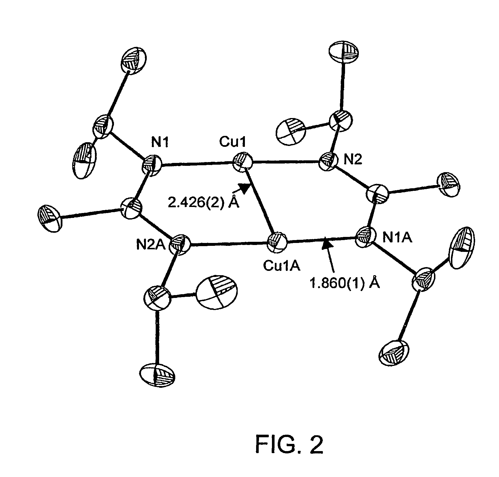
[0077] Co(iPr-AMD)2, shown in FIG. 3, is monomeric with two amidinate ligands arranged about each cobalt atom in a distorted tetrahedral environment. The average Co—N distance is 2.012(8) Å. The Co—N—C—N four-membered rings are planar with an imposed mirror plane.

example 3

Synthesis of cobalt bis(N,N′-di-tert-butylacetamidinate) ([Co(tBu-AMD)2])

[0078] This compound was obtained in a manner similar to ([Co(iPr-AMD)2]) in Example 2, using 1,3-di-tert-butylcarbodiimide in place of 1,3-diisopropylcarbodiimide. Dark blue crystals (84%). Sublimation: 45° C. at 50 mtorr. m.p.: 90° C. Anal. Calcd for C20H42N4Co: C, 60.43; H, 10.65; N, 14.09. Found: C, 58.86; H, 10.33; N, 14.28.


PUM

PropertyMeasurementUnit
Thicknessaaaaaaaaaa
Compositionaaaaaaaaaa
Volatilityaaaaaaaaaa

Abstract

Metal films are deposited with uniform thickness and excellent step coverage. Copper metal films were deposited on heated substrates by the reaction of alternating doses of copper(I) NN′-diisopropylacetamidinate vapor and hydrogen gas. Cobalt metal films were deposited on heated substrates by the reaction of alternating doses of cobalt(II) bis(N,N′-diisopropylacetamidinate) vapor and hydrogen gas. Nitrides and oxides of these metals can be formed by replacing the hydrogen with ammonia or water vapor, respectively. The films have very uniform thickness and excellent step coverage in narrow holes. Suitable applications include electrical interconnects in microelectronics and magnetoresistant layers in magnetic information storage devices.

Description

BACKGROUND OF THE INVENTION [0001] 1. Field of the Invention [0002] This invention relates to materials and processes for deposition of conformal films containing metals on solid substrates, and in particular, to films including copper, cobalt and iron metals or their oxides or nitrides. This invention may be applied to the fabrication of microelectronics devices. [0003] 2. Description of the Related Art [0004] As the speed and functionality of semiconductor microelectronic devices are improved, new materials are needed. For example, materials with higher electrical conductivity are needed to form the wiring between transistors in integrated circuits. Copper has higher electrical conductivity and better stability against electro-migration than does aluminum. Therefore, copper is becoming more commonly used in silicon semiconductors. This trend is described in the International Technology Roadmap for Semiconductors, published on the Internet at http: / / public.itrs.net / Files / 2001ITRS / H...

Claims


Application Information

Patent Timeline
IPC IPC(8): C23C16/40B05D3/02C23C16/34C23C16/18C23C16/44C23C16/455
CPCC07C257/14C23C16/18C23C16/40C23C16/45553C23C16/404C23C16/406C23C16/403C23C16/06C23C16/45525C07C237/00C07F19/00
Inventor GORDON, ROYGLIM, BOOYONGS
Owner PRESIDENT & FELLOWS OF HARVARD COLLEGE
Why Eureka
Try Eureka