Semiconductor device including gate insulation film that is formed of pyroceramics, and method of manufacturing the same
- Summary
- Abstract
- Description
- Claims
- Application Information
AI Technical Summary
Benefits of technology
Problems solved by technology
Method used
Image

Examples
first embodiment
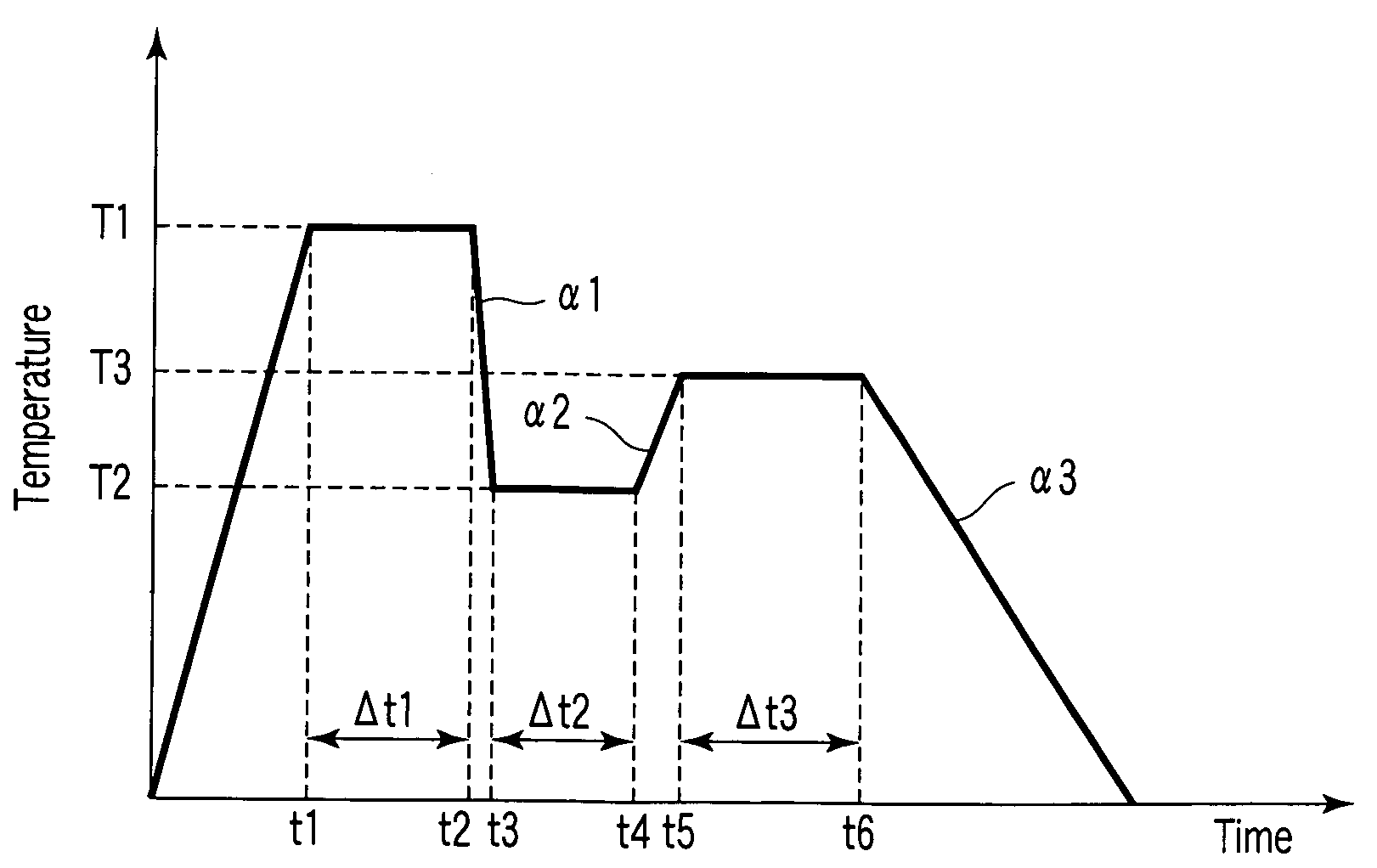
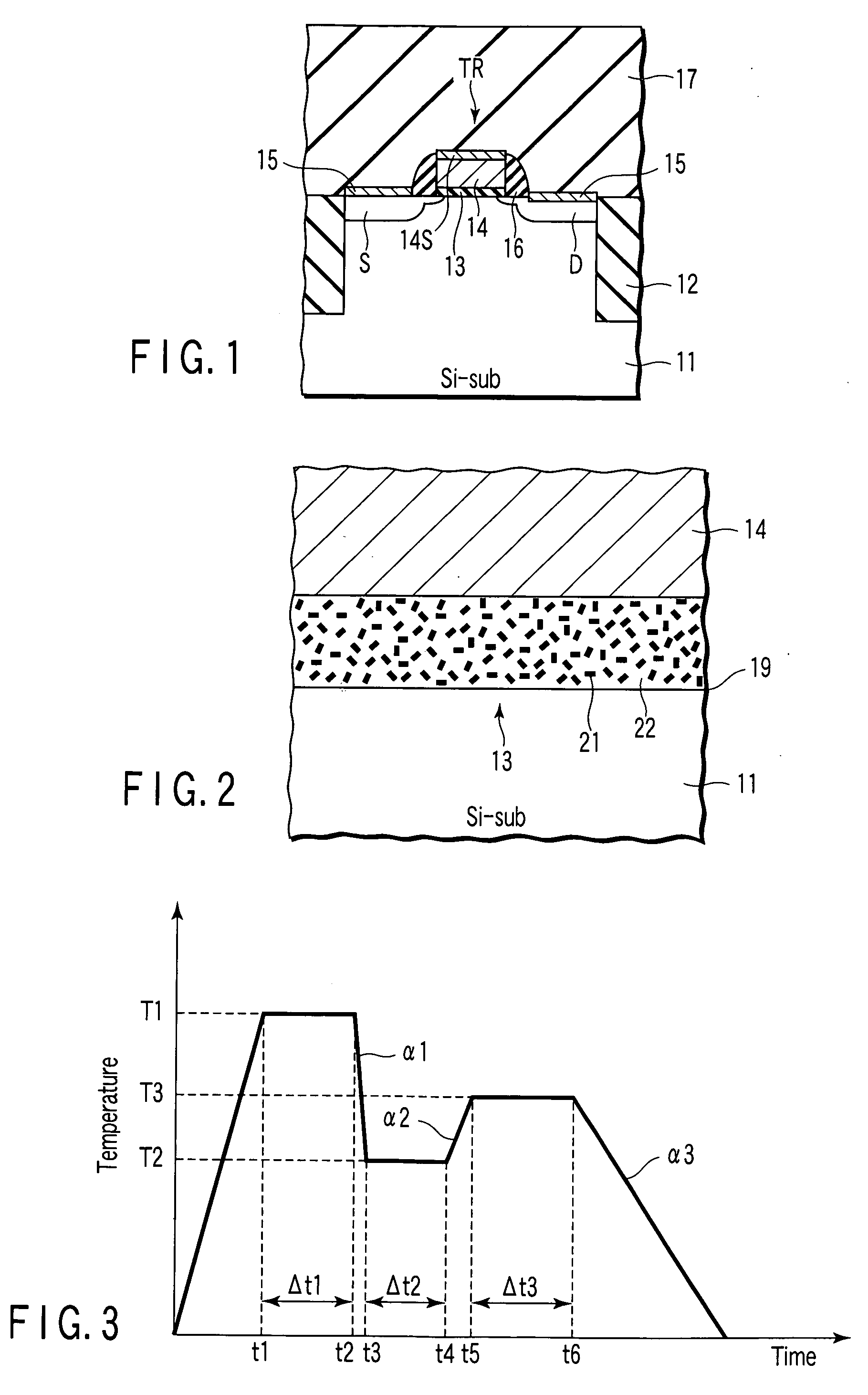
[0026] A semiconductor device according to the first embodiment of the present invention is described with reference to FIG. 1 and FIG. 2. FIG. 1 is a cross-sectional view that schematically shows the semiconductor device according to the first embodiment. FIG. 2 is a cross-sectional view that shows, in enlarged scale, the structure of a gate insulation film 13 shown in FIG. 1.
[0027] As is shown in FIG. 1, a gate-insulated field-effect transistor TR is provided in a device region, which is isolated by a device isolation film 12 that is provided on a major surface of a silicon substrate 11. The transistor TR comprises a gate insulation film 13 provided on the substrate 11, a gate electrode 14 provided on the gate insulation film 13, a silicide layer 14S provided on the gate electrode 14, a source S and a drain D provided in the substrate 11 so as to sandwich the gate electrode 14, silicide layers 15 provided on the source S and drain D, and spacers 16 provided on side walls of the g...
second embodiment (
Ion Implantation Process)
[0079] A method of manufacturing a semiconductor device according to a second embodiment of the invention is described with reference to FIG. 10 and FIG. 11. A description of the parts that are common to those in the first embodiment is omitted.
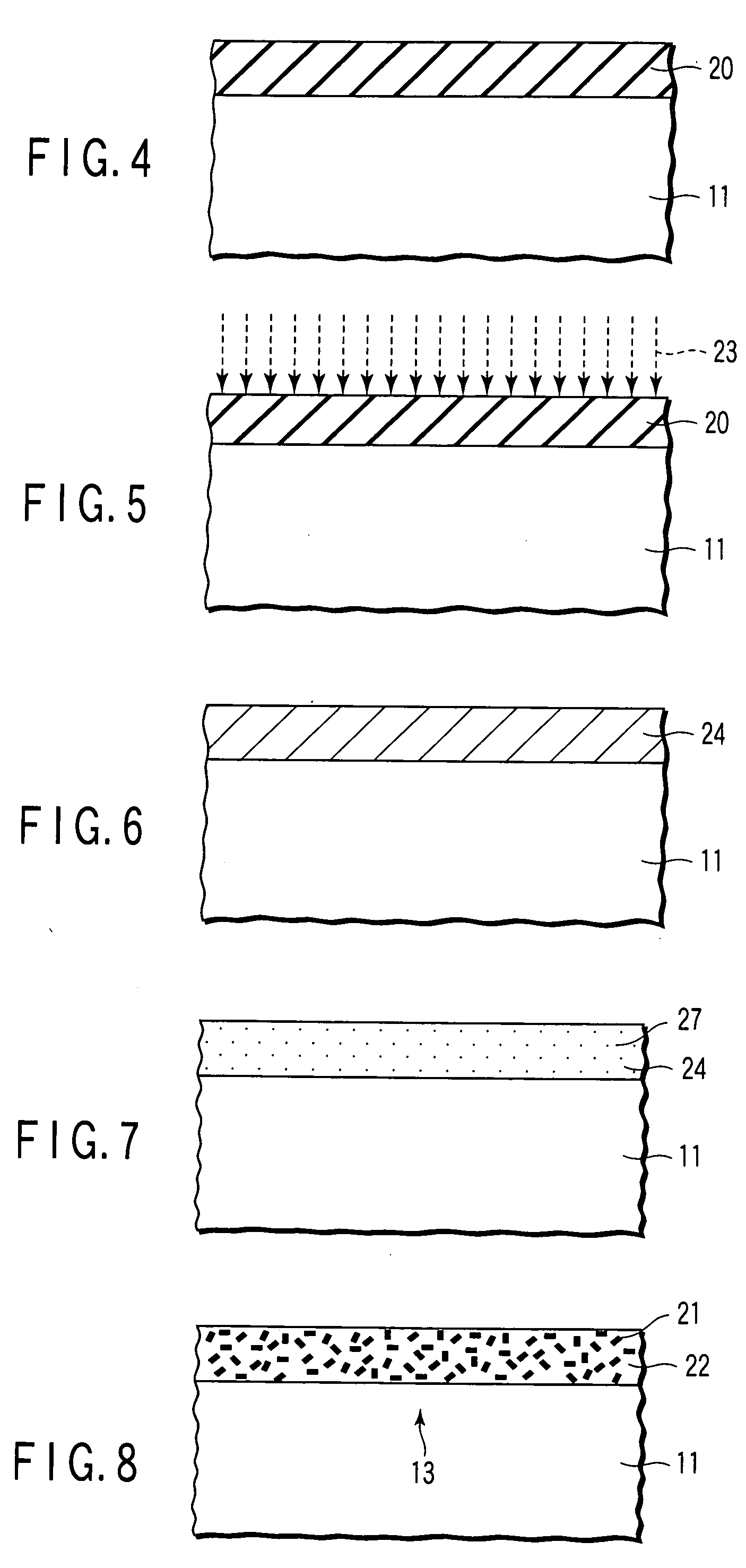
[0080] As is shown in FIG. 10, ion species 23 such as Ba, Ti or Al, are directly implanted into the silicon substrate 11 by, e.g. an ion implantation process, down to a depth 41 that is equal to a necessary thickness of a gate insulation film 13.
[0081] Subsequently, as shown in FIG. 11, the substrate 11 is heated at about 1,000° C. in an oxygen atmosphere by, e.g. a thermal oxidation process. Thus, a silicon oxide film (SiO2 film) 20 including the ion species 23 is formed.
[0082] Then, using the same fabrication steps as in the first embodiment, the semiconductor device shown in FIG. 1 and FIG. 2 can be manufactured.
[0083] According to this manufacturing method, the same advantageous effects as with the first embod...
third embodiment (
Laser Evaporation Process)
[0084] A method of manufacturing a semiconductor device according to a third embodiment of the invention is described with reference to FIG. 12. A description of the parts that are common to those in the first embodiment is omitted. FIG. 12 is a view that schematically illustrates a fabrication step of the semiconductor device according to the third embodiment of the invention.
[0085] To start with, as shown in FIG. 12, oxide powder of, e.g. SiO2, BaTiO3 or Al2O3 is uniformly mixed with a necessary composition. The mixture is sintered, and a ceramics target 51 in a pellet form is fabricated.
[0086] Subsequently, a laser beam 55 is applied from a light source 54 to the target 51, thereby heating the target 51. A plume 52 of the oxide powder emanates from the ablated target 51. Following the above, the plume 52 of the oxide powders is evaporated and deposited on the major surface of the semiconductor substrate 11. Thus, an amorphous layer 24 is formed. Therea...
PUM
 Abstract
Description
Claims
Application Information
 - Generate Ideas
- Intellectual Property
- Life Sciences
- Materials
- Tech Scout
- Unparalleled Data Quality
- Higher Quality Content
- 60% Fewer Hallucinations
Browse by: Latest US Patents, China's latest patents, Technical Efficacy Thesaurus, Application Domain, Technology Topic, Popular Technical Reports.
© 2025 PatSnap. All rights reserved.Legal|Privacy policy|Modern Slavery Act Transparency Statement|Sitemap|About US| Contact US: help@patsnap.com