Check patentability & draft patents in minutes with Patsnap Eureka AI!

Switching element method of driving switching element rewritable logic integrated circuit and memory

a technology of switching element and integrated circuit, which is applied in the direction of digital storage, semiconductor devices, instruments, etc., can solve the problems of not being able to reprogramme, not meeting the requirements and failing to meet the demands of debugging the program while it is in operation, etc., to achieve small resistance, small design, and high speed

Active Publication Date: 2006-07-27
NEC CORP
View PDF5 Cites 68 Cited by
  • Summary
  • Abstract
  • Description
  • Claims
  • Application Information

AI Technical Summary

Benefits of technology

[0014] It is an object of the present invention to provide a switching element which can be highly integrated, can be kept in either one of an on state and an off state even when the switching element is switched off, has a low resistance when it is in the on state, and can be reprogrammed into either one of the on and off states, a method of driving the switching element, and an FPL circuit and a memory element which employ the switching element.

Problems solved by technology

However, the antifuse element is problematic in that it is not reprogrammable.
Consequently, when the FPL circuit is programmed, it fails to meet demands for debugging the program and changing programs while it is in operation.
While the EEPROM as the second conventional example is reprogrammable, the level of integration thereof is low at present and the on-resistance thereof is of a large value of several kΩ because it is limited by the resistance of the MOS (Metal Oxide Semiconductor) transistor.
Though the EEPROM is widely used as nonvolatile memory, the level of integration thereof is limited by the thickness of the insulating film, making it difficult to further integrate the EEPROM.
In addition, when the EEPROM is used in an FPL circuit, it tends to cause a signal delay due to the large on-resistance.
The timer cannot operate as a switching element for switching between on and off states.
When the transition occurs between the on and off states, a current flows through the switch, and the switch consumes a large amount of electric power.
Even though the switch itself can be integrated, it is difficult to integrate the interconnects and peripheral circuits.

Method used


Image

  • Switching element method of driving switching element rewritable logic integrated circuit and memory
  • Switching element method of driving switching element rewritable logic integrated circuit and memory
  • Switching element method of driving switching element rewritable logic integrated circuit and memory

Examples


1st embodiment

[0102] Of switching elements according to the present invention, a switching element employing a solid electrolyte as an ion conductor will be described below.

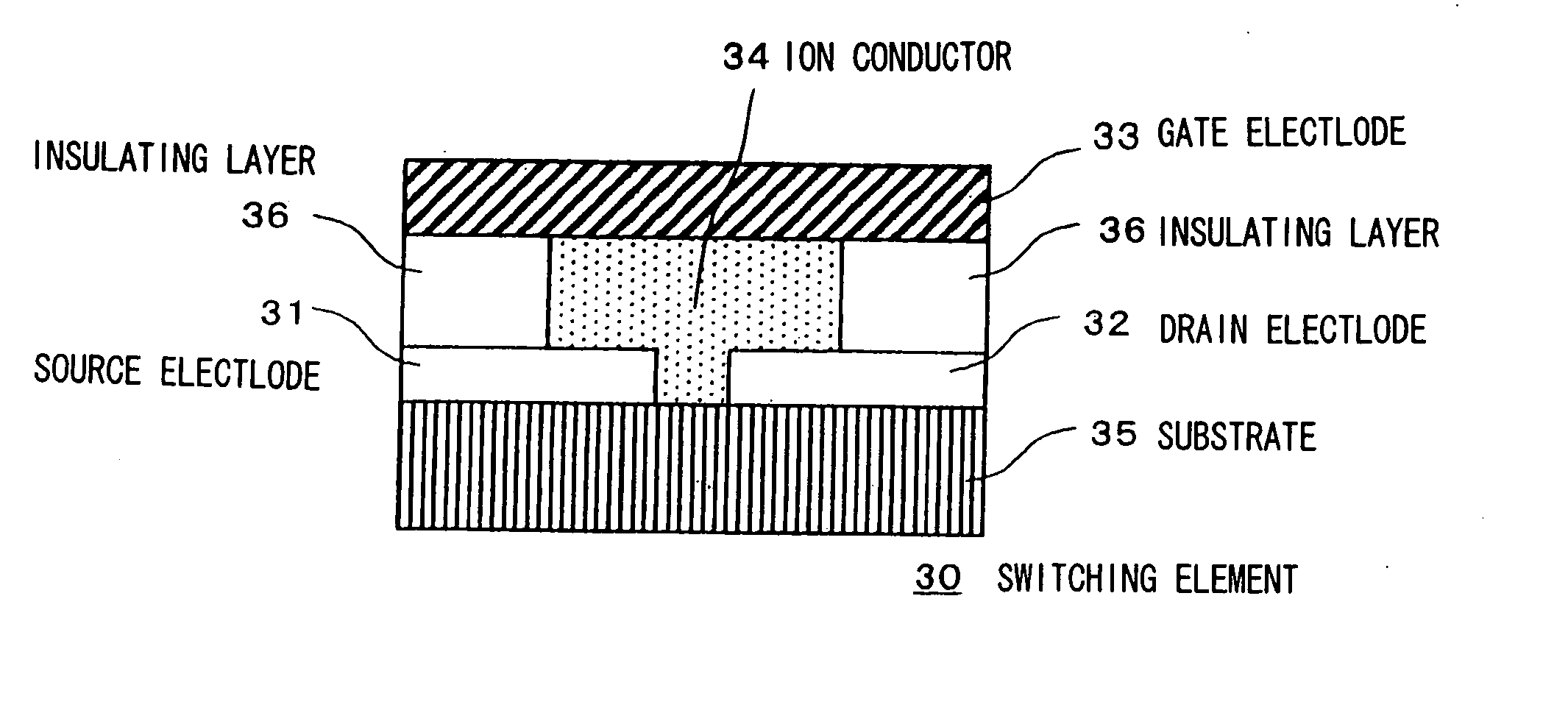
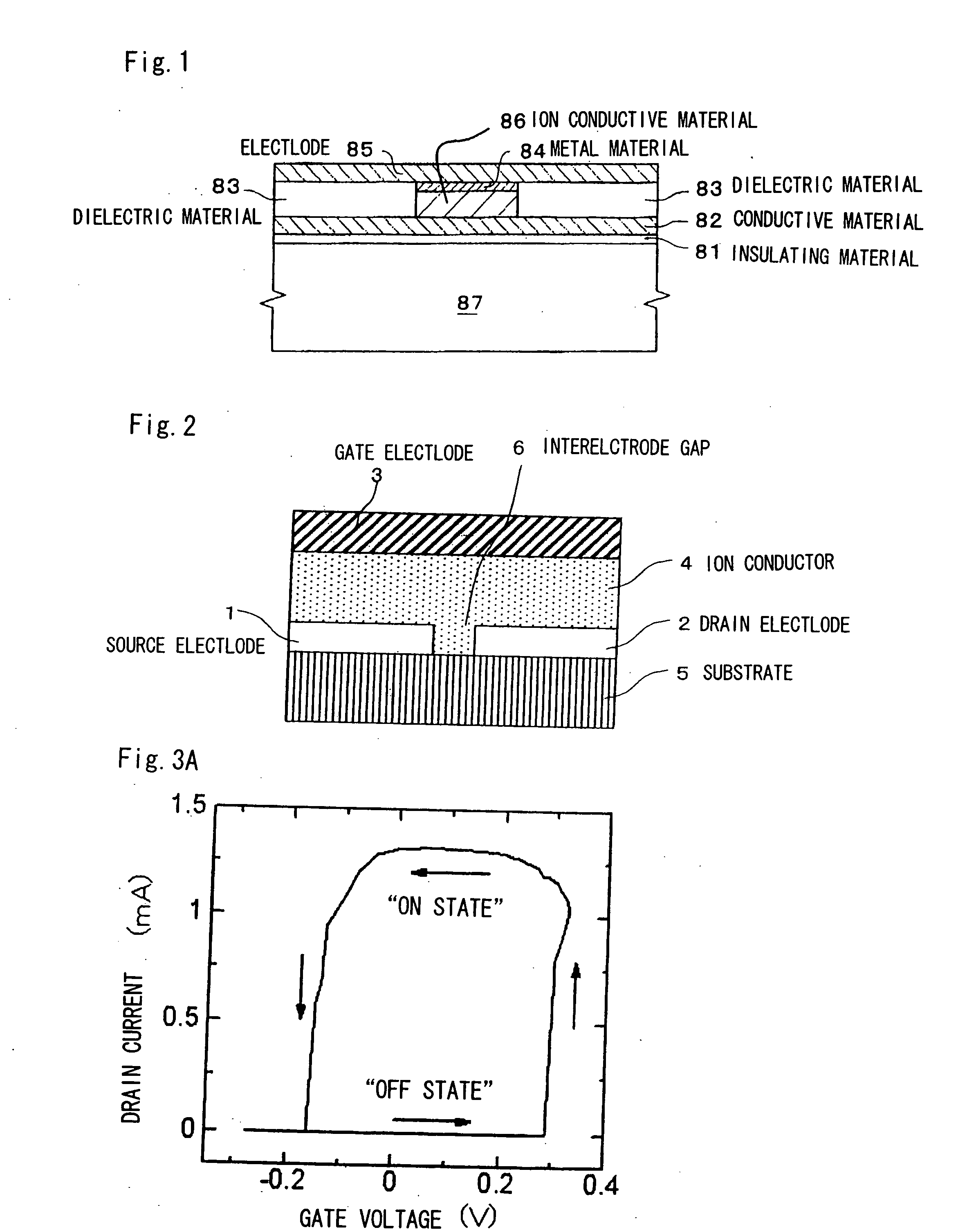
[0103]FIG. 5 is a cross-sectional view of the structure of a switching element according to the present invention. As shown in FIG. 5, switching element 10 has gate electrode 13 disposed on substrate 15 covered with a silicon oxide film as an insulating film, ion conductor 14 disposed on gate electrode 13, and source electrode 11 and drain electrode 12 disposed on ion conductor 14. Source electrode 11 and drain electrode 12 are disposed within one plane, with a gap of 100 nm or less defined therebetween. Source electrode 11, drain electrode 12, and gate electrode 13 are electrically insulated from each other.

[0104] Gate electrode 13 includes a material for supplying metal ions to ion conductor 14 based on an electrochemical reaction. Ion conductor 14 should preferably comprise a solid electrolyte with as small electron condu...

2nd embodiment

[0131] The present embodiment is characterized in that the drain electrode in the first embodiment is formed of the same material as that of the gate electrode.

[0132] An arrangement of the switching element according to the present embodiment will be described below.

[0133]FIG. 11 is a cross-sectional view of a structure of the switching element according to the present embodiment.

[0134] As shown in FIG. 11, switching element 50 has gate electrode 53 disposed on substrate 55 covered with an insulating film, ion conductor 54 disposed on gate electrode 53, and source electrode 51 and drain electrode 52 disposed on ion conductor 54. Source electrode 51, drain electrode 52, and gate electrode 53 are electrically insulated from each other.

[0135] Source electrode 51 and drain electrode 52 are disposed within one plane. Gate electrode 53 and drain electrode 52 include a material for supplying metal ions to ion conductor 54 based on an electrochemical reaction. Each of source electrode 5...

3rd embodiment

[0149] An arrangement of an FPL circuit which incorporates switching elements according to the present invention will be described below.

[0150] As described in the background art, the FPL circuit has a plurality of logic circuit blocks, interconnects that interconnect the logic circuit blocks, and antifuse elements for changing the connection of the interconnects. According to the present embodiment, switching elements according to the present invention are used as programming elements instead of as antifuse elements.

[0151]FIG. 12 is a cross-sectional view showing a structure of a switching element according to the present invention as it is applied to an FPL circuit.

[0152] The structure shown in FIG. 12 is similar to the first embodiment shown in FIG. 8A except that source electrode 21 in FIG. 8A is replaced with interconnect A61 and drain electrode 22 in FIG. 8A is replaced with interconnect B62.

[0153] Operation of the switching element shown in FIG. 12 will be described below...


PUM


Abstract

A switching element has an ion conductor capable of conducting metal ions for use in an electrochemical reaction therein, a first electrode and a second electrode which are disposed in contact with said ion conductor and spaced a predetermined distance from each other, and a third electrode disposed in contact with the ion conductor. When a voltage for causing the switching element to transit to an on state is applied to the third electrode, metal is precipitated between the first electrode and the second electrode by metal ions, electrically interconnecting the first electrode and the second electrode, When a voltage for causing the switching element to transit to an off state is applied to the third electrode, the precipitated metal is dissolved to electrically disconnect the first electrode and the second electrode from each other.

Description

TECHNICAL FIELD [0001] The present invention relates to a switching element utilizing an electrochemical reaction, a method of driving the switching element, an FPL (Field Programmable Logic: a rewritable logic integrated circuit) circuit and a memory element which employ the switching element. BACKGROUND ART [0002] Of memory integrated circuits, switching elements having a non-volatile function capable of being kept on or off even when their power supply is switched off include an antifuse element as a first conventional example and an EEPROM (Electrical Erasable Programmable Read Only Memory) as a second conventional example. [0003] Switching elements for performing a nonvolatile function based on an electrochemical reaction include a timer (or an electrochemical time switching device) as a third conventional example and a PCRAM (Programmable Conductor Random Access Memory) as a fourth conventional example. [0004] The antifuse element as the first conventional example is a switchi...

Claims


Application Information

Patent Timeline
IPC IPC(8): G11C11/00G11C13/02H01L27/10H01L45/00
CPCG11C13/0011G11C13/0069G11C2013/009G11C2213/15G11C2213/79H01L27/101H01L27/2436H01L45/085H01L45/1206H01L45/1266H01L45/142H01L45/1633H10B63/30H10N70/253H10N70/245H10N70/8416H10N70/8822H10N70/028H01L21/82H01L29/66
Inventor SAKAMOTO, TOSHITSUGUKAWAURA, HISAOSUNAMURA, HIROSHI
Owner NEC CORP
Features
  • R&D
  • Intellectual Property
  • Life Sciences
  • Materials
  • Tech Scout
  • Unparalleled Data Quality
  • Higher Quality Content
  • 60% Fewer Hallucinations
Learn More