Method for forming inorganic thin film pattern on polyimide resin

a polyimide resin and inorganic technology, applied in the direction of liquid/solution decomposition chemical coating, coating, printed circuit aspects, etc., can solve the problems of high cost, low productivity, and generation of many useless metal materials, and achieve high pattern precision and high reliability

Inactive Publication Date: 2006-07-27
MITSUBOSHI BELTING LTD +1
View PDF4 Cites 31 Cited by
  • Summary
  • Abstract
  • Description
  • Claims
  • Application Information

AI Technical Summary

Benefits of technology

[0031] In accordance with the present invention, an alkaline aqueous solution is made to act only on the concave part which is not coated with an alkali-resistant protective film so that carboxyl group is produced in the polyimide resin, and a metal or a metal oxide or a semiconductor is separated on the inner surface of the concave part so that the inorganic thin film is able to be formed, and formation of the inorganic thin film is able to be done in the concave part of the site where the pattern is formed. Thus, the inorganic thin film is able to be formed in a high reliability for close adhesion and in a high pattern precision.

Problems solved by technology

However, there is a problem that such a method requires an expensive apparatus and, moreover, it has a low productivity and results in a high cost.
Although this subtractive method has an excellent productivity and is useful as a method for forming a circuit pattern relatively easily, many metal films are to be removed in the preparation of a circuit pattern and, therefore, there is a problem that much useless metal material is generated.
In addition, there has been a demand in recent years for much finer circuit pattern as a result of trend of high density of the electronic circuit substrate but, in a subtractive method, there is another problem that, due to generation of over-etching and to the presence of adhesive or unevenness by roughening of the substrate surface, it is difficult to meet the request for formation of a fine circuit pattern.
However, since it is difficult to ensure the adhesive force between the polyimide resin base material and the metal film, there is a problem of inferior reliability for close adhesion.
There is another problem in the additive method that its steps are complicated and an expensive production facility is necessary for formation of fine circuit pattern resulting in a high cost.
However, when metal nano-particle numbers per unit area of the substrate surface are insufficient in spraying and applying of the metal nano-particles by an ink jet system, there is a possibility that the resulting metal film is broken due to shrinking as a result of sintering among the metal nano-particles upon annealing, while when metal nano-particle numbers are in excess, there is a possibility that flatness and smoothness of the metal film formed after the annealing are lost whereby there is a problem that control of applying amount of the metal nano-particles on the substrate is very severe.
In addition, due to their properties, metal component of metal nano-particles and substrate are hardly difficult to achieve a sufficient reliability for close adhesion.
Further, there is another problem in precision of the size due to shrinking as a result of sintering among nano-particles upon annealing.
However, in a method for forming a pattern by irradiation of ultraviolet ray via a photomask as in Reference 1, it is difficult to cope with a very fine circuit pattern being demanded as the trend of high density of the circuit substrate.
However, in a plating method, metal film is separated out in an isotropic manner and, therefore, there is a risk that precision of the pattern is deteriorated after the thickening and, at the same time, reliability for close adhesion lowers.
In order to solve such a problem, there is a proposal, for example, where a high-molecular film is formed on the substrate surface which is other than the site where a circuit pattern is formed and then thickening is conducted by a plating method but there is a problem that steps become complicated resulting in a high cost.

Method used


Image

  • Method for forming inorganic thin film pattern on polyimide resin
  • Method for forming inorganic thin film pattern on polyimide resin
  • Method for forming inorganic thin film pattern on polyimide resin

Examples


example 1

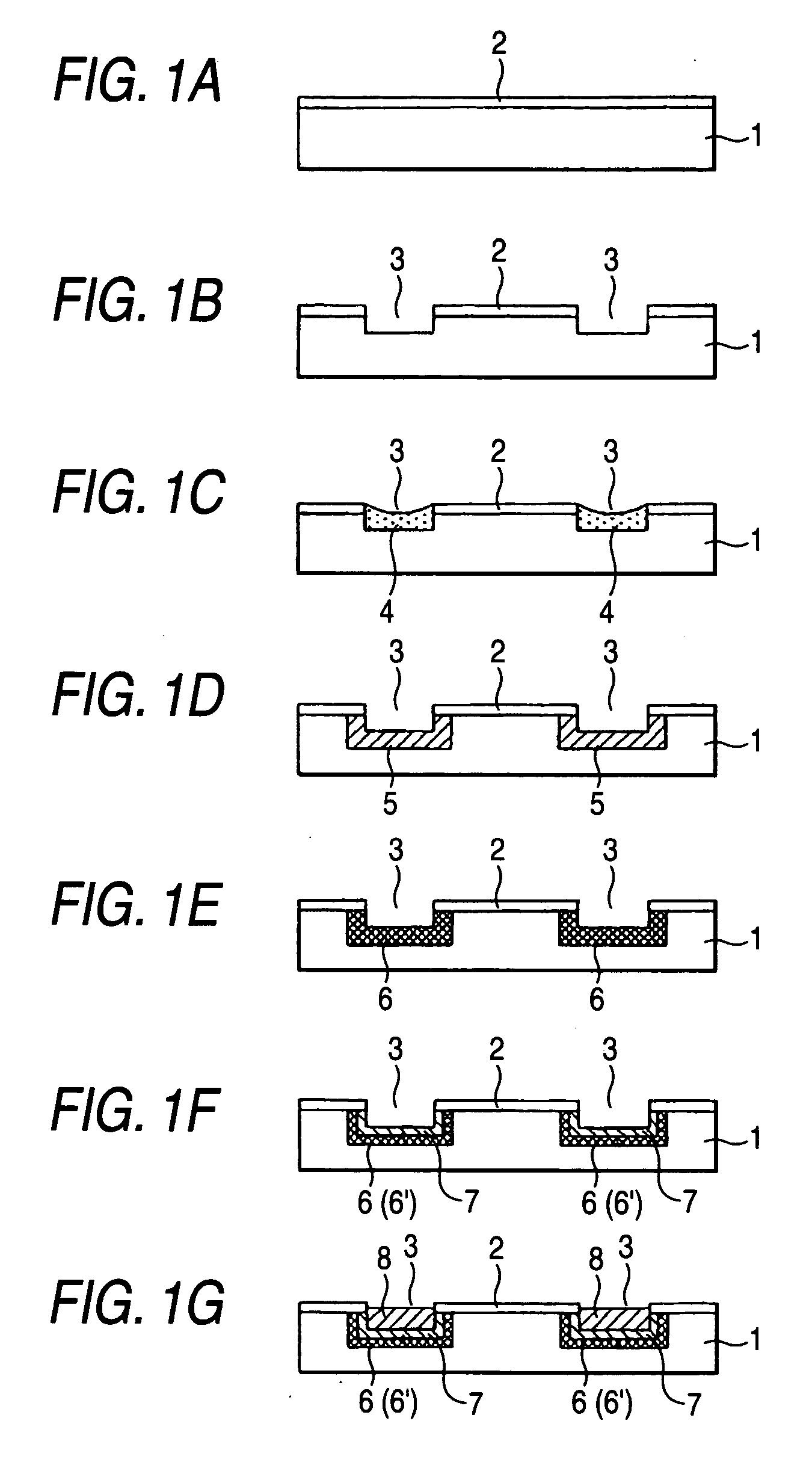
[0067] Polyimide film (manufacture by DuPont-Toray Co., Ltd; trade name: Kapton 200-H) was dipped in an ethanol solution, subjected to an ultrasonic cleaning for 5 minutes and dried in an oven at 100° C. for 60 minutes to clean the surface of the polyimide film.

[0068] In the meanwhile, a polystyrene solution was prepared by dissolving 50 parts by mass of polystyrene in 180 parts by mass of toluene and the polystyrene solution was uniformly applied on the surface of the polyimide film by a spin coating method under the condition of 1,500 rpm for 30 seconds. After that, it was kept for 10 minutes in an oven which was kept at 60° C. to form an alkali-resistant protective film of polystyrene on the polyimide film (refer to FIG. 1A). Film thickness of the alkali-resistant protective film was 0.5 μm.

[0069] Then an ultraviolet laser apparatus was used, a circuit pattern with a line width of 5 μm was drawn under the following conditions and the alkali-resistant protective film and the sup...

example 2

[0075] Acrylate resin (10 parts by mass) was dissolved in 80 parts by mass of terpineol to prepare an acrylate resin paste. Then, the acrylate resin paste was applied by a screen printing method via a screen plate of 300 meshes of SUS and 5 μm of emulsifier on the surface of polyimide film where the surface was cleaned in the same manner as in Example 1 and kept for 30 minutes in an oven of 110° C. to form an alkali-resistant protective film of the acrylate resin on the surface of the polyimide film (refer to FIG. 1A). Film thickness of this alkali-resistant protective film was 10 μm.

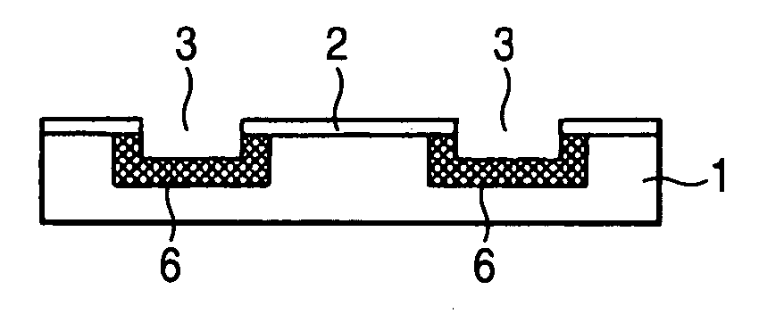
[0076] Then a circuit pattern of line width of 40 μm was drawn under the following condition using a YAG laser apparatus and the alkali-resistant protective film and the superficial portion of the polyimide film were removed to form a concave part in a pattern shape on the polyimide film (refer to FIG. 1B). Depth of the concave part was 18 μm.

Laser output50WWavelength1064nmOscillating operationpulseS...

example 3

[0082] Polypropylene (30 parts by mass) was dissolved in 180 parts by mass of toluene to prepare a polypropylene solution. Then, the polypropylene solution was uniformly applied by a dipping method under the condition of pulling-up speed of 20 mm / second on the polyimide film where the surface was cleaned in the same manner as in Example 1 and kept for 5 minutes in an oven kept at 40° C. to form an alkali-resistant protective film of the polypropylene on the surface of the polyimide film (refer to FIG. 1A). Film thickness of this alkali-resistant protective film was 0.03 μm.

[0083] Then a circuit pattern of line width of 3 μm was drawn under the following condition using a femtosecond laser apparatus and the alkali-resistant protective film and the superficial portion of the polyimide film were removed to form a concave part in a pattern shape on the polyimide film (refer to FIG. 1B). Depth of the concave part was 3 μm.

Laser output10WWavelength780nmOscillating operationpulseScannin...


PUM

PropertyMeasurementUnit
thicknessaaaaaaaaaa
thicknessaaaaaaaaaa
thicknessaaaaaaaaaa

Abstract

The present invention provides 1. A method for forming an inorganic thin film pattern on a polyimide resin, which has: (1) a step of forming an alkali-resistant protective film having a thickness of 0.01 to 10 μm on a surface of a polyimide resin; (2) a step of removing the alkali-resistant protective film and a superficial portion of the polyimide resin at the site where an inorganic thin film pattern is formed to form a concave part; (3) a step of contacting an alkaline aqueous solution to the polyimide resin in the concave part to cleave an imide ring of the polyimide resin so as to produce a carboxyl group whereby a polyimide resin having the carboxyl group is formed; (4) a step of contacting a solution containing a metal ion to the polyimide resin having the carboxyl group so as to produce a metal salt of the carboxyl group; and (5) a step of separating the metal salt as a metal, a metal oxide or a semiconductor on the surface of the polyimide resin so as to form the inorganic thin film pattern.

Description

FIELD OF THE INVENTION [0001] The present invention relates to a method for forming an inorganic thin film pattern on a polyimide resin where an inorganic thin film is formed on a surface of a polyimide resin in a fine pattern such as a circuit pattern. BACKGROUND OF THE INVENTION [0002] Various methods have been proposed for a method of forming a circuit pattern on the surface of a base material made by polyimide resin such as polyimide film. Among them, a dry process such as vacuum evaporation method and sputtering method have been known as a method which is able to well form a fine circuit pattern having an excellent reliability for close adhesion. However, there is a problem that such a method requires an expensive apparatus and, moreover, it has a low productivity and results in a high cost. [0003] Therefore, as a most common method for forming a circuit pattern, a subtractive method where the whole surface of the polyimide resin base material is coated with a metal film to pre...

Claims


Application Information

Patent Timeline
Patent Type & Authority Applications(United States)
IPC IPC(8): B05D3/00B05D5/12
CPCC23C18/04C23C18/06C23C18/08C23C18/1216C23C18/1245C23C18/1275C23C18/1295H05K1/0346H05K3/0032H05K3/107H05K3/184H05K3/381H05K2201/0154H05K2201/0326H05K2203/0793H05K2203/1157H05K2203/1163
Inventor YANAGIMOTO, HIROSHINAWAFUNE, HIDEMIAKAMATSU, KENSUKE
Owner MITSUBOSHI BELTING LTD
Why Eureka
Try Eureka