Semiconductor device and manufacturing method thereof

a technology of semiconductor devices and manufacturing methods, applied in the direction of semiconductor devices, basic electric elements, electrical appliances, etc., can solve the problems of low thermal stability and low dielectric constant, easy oxidization of metals undesirably reacting with high-k films, etc., and achieve the effect of reducing leak current and eo

Active Publication Date: 2006-08-03
KIOXIA CORP
View PDF1 Cites 11 Cited by
  • Summary
  • Abstract
  • Description
  • Claims
  • Application Information

AI Technical Summary

Benefits of technology

[0010] An advantage of an aspect of the present invention is to provide a semiconductor device having a gate insulator suppressed in thermal reaction with a semiconductor layer and in thermal reaction with a gate electrode, and thereby reduced in leak current and EOT.

Problems solved by technology

Although germanium is thermodynamically less reactive with High-k films than silicon, it forms a GeO2 layer, which is low in thermal stability and low in dielectric constant, along the interface between such a High-k film and the germanium substrate.
Furthermore, easy-to-oxidize metals undesirably react with High-k films.
This results in increasing the leak current and degrading the reliability.

Method used


Image

  • Semiconductor device and manufacturing method thereof
  • Semiconductor device and manufacturing method thereof
  • Semiconductor device and manufacturing method thereof

Examples


first embodiment

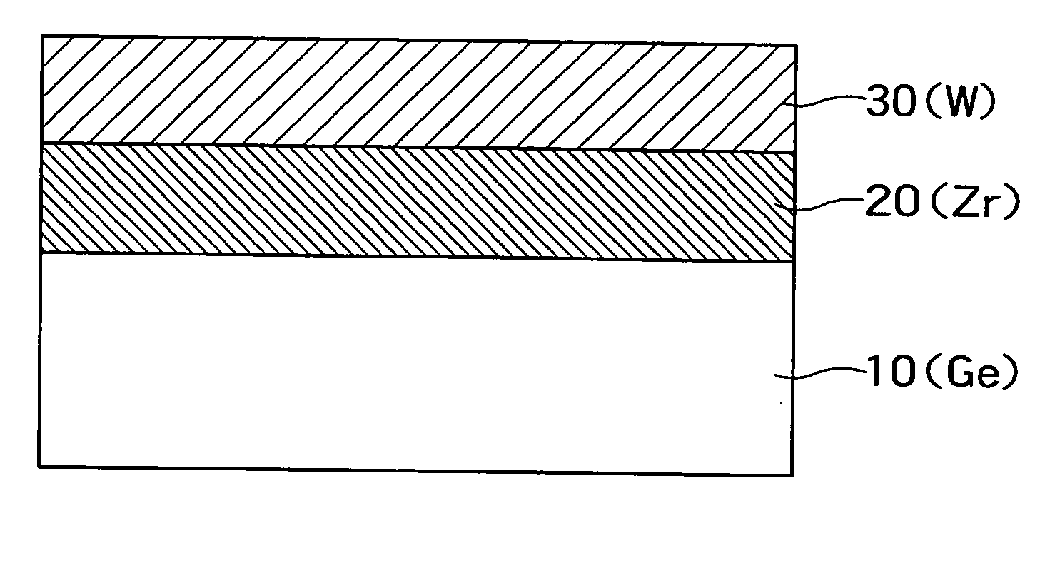
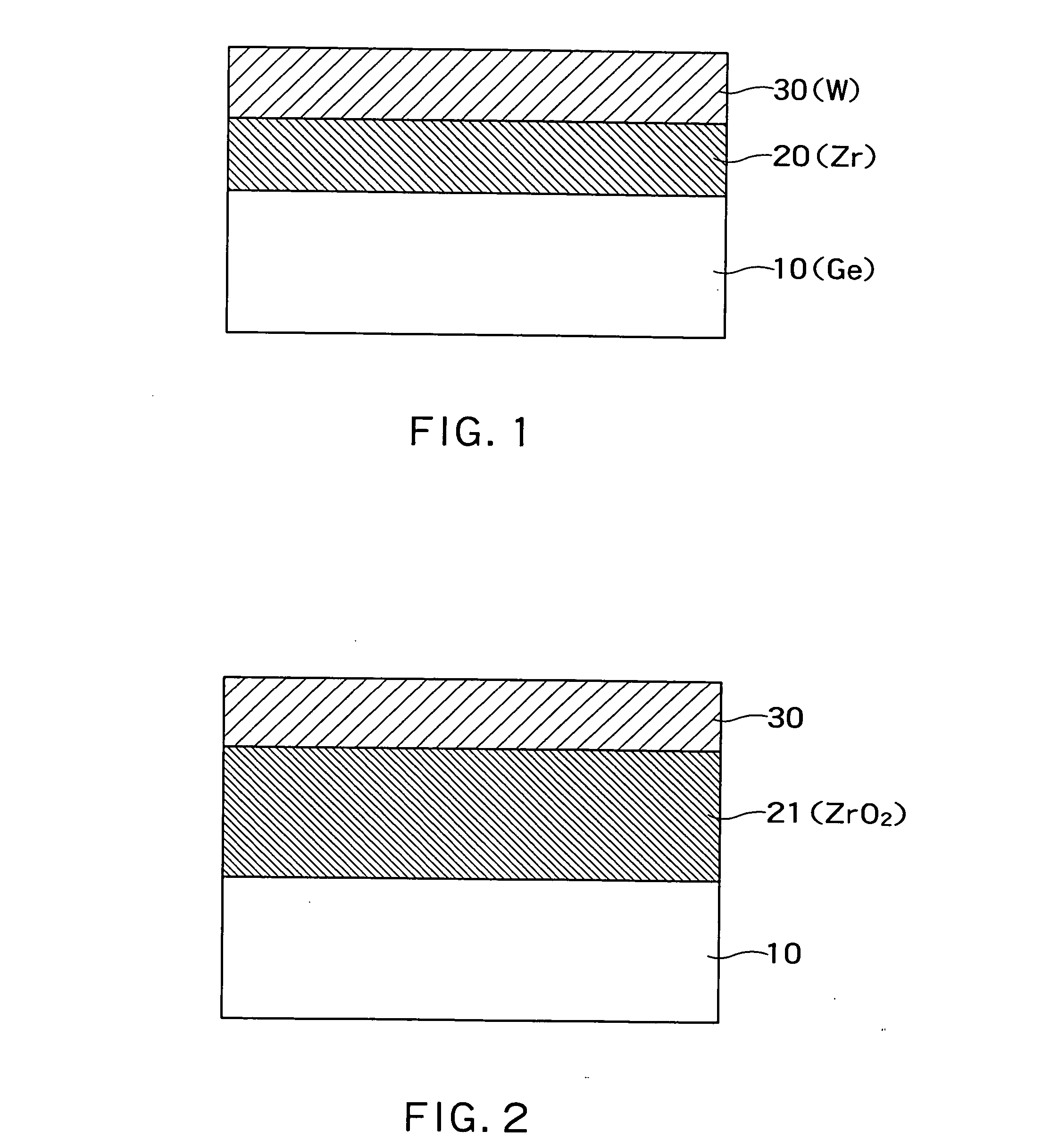
[0036]FIGS. 1 and 2 are cross-sectional views showing a manufacturing method of a semiconductor device according to the first embodiment of the invention. This embodiment is directed to a manufacturing method of a semiconductor device having a MIS (Metal Insulator Semiconductor) structure.

[0037] A natural oxide film is removed from the surface of a single-crystal germanium (Ge) substrate 10. As shown in FIG. 1, next deposited on the germanium substrate 10 is a zirconium film 20 as a first material for a gate insulator. Subsequently, a tungsten (W) film 30 is deposited as a second material for a gate electrode on zirconium film 20. Thickness of the tungsten film 30 is preferably equal to or less than 20 nm to permit hydrogen and oxygen to diffuse into the zirconium film 20 through the tungsten film 30. This will be explained later in greater detail with reference to FIGS. 16 and 17. For example, the zirconium film 20 and the tungsten film 30 may be 2 nm thick approximately.

[0038] A...

second embodiment

[0060]FIGS. 4 and 5 are cross-sectional views showing a method of manufacturing a semiconductor device according to the second embodiment of the invention. As shown in FIG. 4, the zirconium oxide (ZrO2) film 21 as the first material for the gate insulator is deposited on the germanium substrate 10. After that, the tungsten film 30 as the second material for the gate insulator is deposited on the zirconium oxide (ZrO2) film 21.

[0061] In the second embodiment, since the zirconium oxide (ZrO2) film 21 is deposited as the first material for the gate insulator, the first material for the gate insulator need not be oxidized selectively. However, once an oxide is deposited on the germanium substrate, the surface of the germanium substrate 10 is undesirably oxidized. As a result, as shown in FIG. 5, a germanium oxide (GeO2) film 11 is undesirably formed between the germanium substrate 10 and the zirconium oxide film 21. Since the germanium oxide film 11 has a dielectric constant lower than...

third embodiment

[0067]FIGS. 6 and 7 are cross-sectional views showing a manufacturing method of a semiconductor device according to the third embodiment of the invention. As shown in FIG. 6, a hafnium oxide (HfO2) film 51 is first deposited as the first material for the gate insulator on the germanium substrate 10. Subsequently, the tungsten (W) film 30 is deposited as the second material for the gate electrode on the hafnium oxide film 51. The hafnium oxide film 51 and the tungsten film 30 may be approximately 2 nm thick respectively.

[0068] Once the hafnium oxide film 51 is deposited on the germanium substrate, the germanium oxide (GeO2) film 11 is undesirably formed along the interface between the germanium substrate 10 and the hafnium oxide film 51. For example, if the thickness of the hafnium oxide film 51 is 2 nm, the germanium oxide film 11 becomes 3 nm thick approximately. The germanium oxide film 11 has a lower dielectric constant than the hafnium oxide film 51. Therefore, EOT of the gate ...


PUM

PropertyMeasurementUnit
temperatureaaaaaaaaaa
thicknessaaaaaaaaaa

Abstract

A method of manufacturing a semiconductor device includes forming a semiconductor layer containing a semiconductor material having a first oxide-generating Gibbs free energy required to become an oxide; forming a first material for a gate insulator on the semiconductor layer, said first material containing an element having a second oxide-generating Gibbs free energy required to become an oxide and becoming insulative when the element is oxidized or nitrided; and annealing the first material in an atmosphere containing hydrogen atoms, or heavy hydrogen atoms, and oxygen atoms in a temperature range where the first oxide-generating Gibbs free energy is equal to or higher than the second oxide-generating Gibbs free energy.

Description

CROSS-REFERENCE TO RELATED APPLICATION [0001] This application is based upon and claims the benefit of priority from the prior Japanese Patent Applications No. 2005-20942, filed on Jan. 28, 2005, the entire contents of which are incorporated herein by reference. BACKGROUND OF THE INVENTION [0002] 1. Field of the Invention [0003] The present invention relates to a semiconductor device and a manufacturing method thereof. [0004] 2. Background Art [0005] Along with microminiaturization of semiconductor integrated circuits, MIS semiconductor elements are getting more and more miniaturized. ITRS (International Technology Roadmap for Semiconductors), 2003 Edition, predicts that EOT (Equivalent Physical Oxide Thickness) of gate insulators will be reduced to 0.7 nm or less in 2010 or later. To prevent leak current while employing so thin gate insulators thinned to this level, the use of highly dielectric metal insulators (High-k films) such as ZrO2 and HfO2 will be indispensable. [0006] High...

Claims


Application Information

Patent Timeline
Patent Type & Authority Applications(United States)
IPC IPC(8): H01L29/78H01L21/4763
CPCH01L21/28255H01L29/513H01L29/517
Inventor MURAOKA, KOICHI
Owner KIOXIA CORP
Why Eureka
Try Eureka