One-transistor random access memory technology integrated with silicon-on-insulator process

a random access memory and silicon-on-insulator technology, applied in the field of one-transistor random access memory (itram) technology, can solve the problems of low speed, high power consumption, insufficient capacitance, and conventional 1t-ram cells, and achieve low power consumption, moderate capacitance, and high speed operation.

Inactive Publication Date: 2006-08-03
TAIWAN SEMICON MFG CO LTD
View PDF5 Cites 24 Cited by
  • Summary
  • Abstract
  • Description
  • Claims
  • Application Information

AI Technical Summary

Benefits of technology

[0005] These and other problems are generally solved or circumvented, and technical advantages are generally achieved, by preferred embodiments of the present invention that utilize an one-transistor random access memory process integrated with a silicon-on-insulator (SOI) process. Such the SOI-based 1T-RAM device brings advantages of high-speed operation, low-power consumption and moderate capacitance, improves soft-error and latch-up immunity, and contributes to a long static retention time.

Problems solved by technology

The conventional 1T-RAM cell, however, has disadvantages of low speed, high power consumption and insufficient capacitance.

Method used


Image

  • One-transistor random access memory technology integrated with silicon-on-insulator process
  • One-transistor random access memory technology integrated with silicon-on-insulator process
  • One-transistor random access memory technology integrated with silicon-on-insulator process

Examples


Embodiment Construction

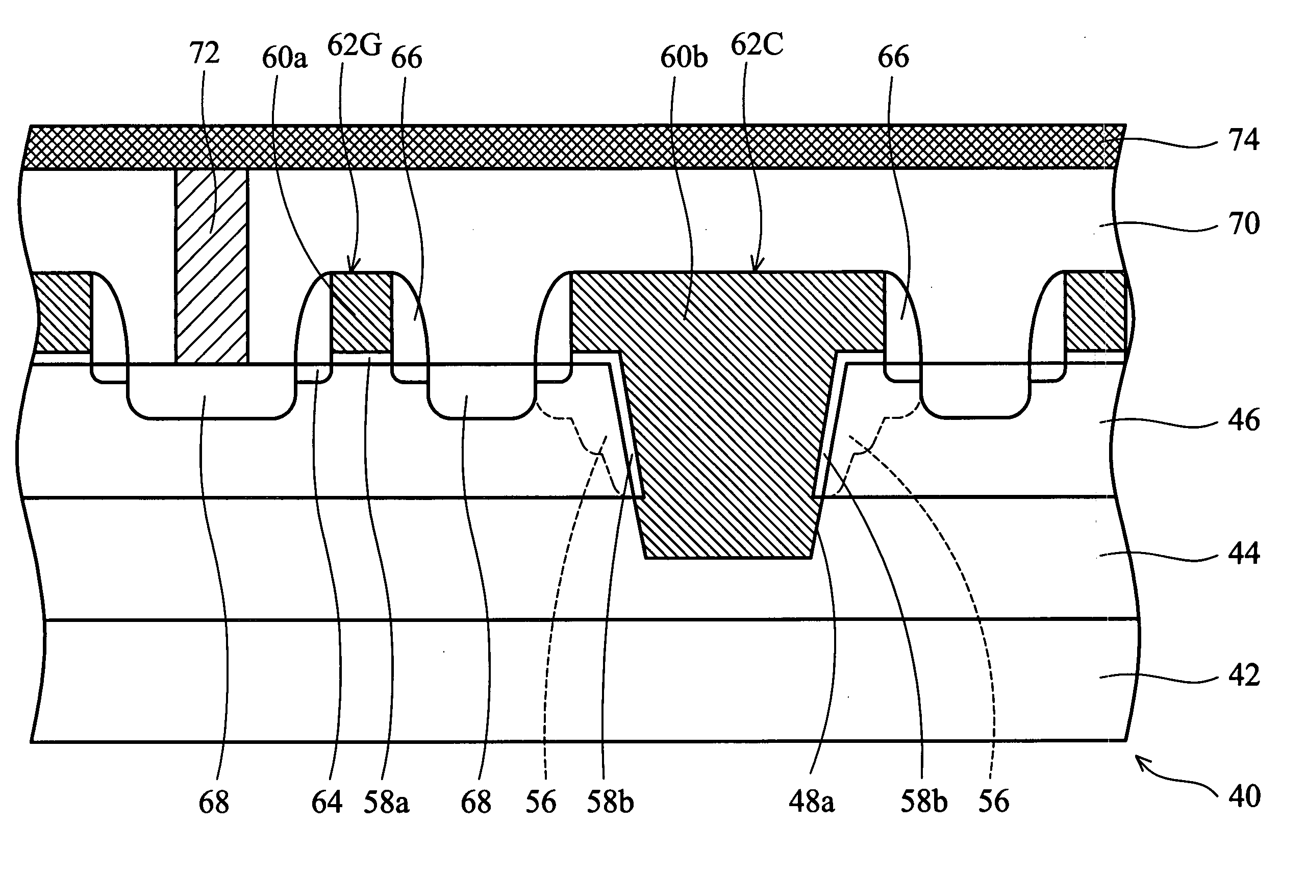
[0012] The present invention provides a 1T-RAM technology integrated with a SOI process, referred to as a SOI-based 1T-RAM process, to form a 1T-RAM device on a SOI substrate, which overcomes the problems of the prior art arising from the use of silicon bulk substrate. Such the SOI-based 1T-RAM device brings advantages of high-speed operation, low-power consumption and moderate capacitance, improves soft-error and latch-up immunity, and contributes to a long static retention time. The SOI-based 1T-RAM process has wide applicability to many manufacturers, factories and industries and is potentially suited to a wide range of semiconductor device applications, for example mixed-mode integrated circuits, radio frequency (RF) circuits, static random access memory (SRAM), and dynamic random access memory (DRAM) technologies. The SOI-based 1T-RAM device may be built in a system-on-chip (SOC) including memory cell (e.g., DRAM, SRAM, Flash, EEPROM and EPROM), logic, analog and I / O devices. F...


PUM


Abstract

An one-transistor random access memory device integrated on a silicon-on-insulator (SOI) substrate has a capacitor structure buried in at least part of a capacitor trench in the SOI substrate, and a gate structure formed on the SOI substrate. A top electrode the capacitor structure is formed simultaneously with and of the same conductive material as a gate electrode of the gate structure. A capacitor dielectric layer of the capacitor structure is formed simultaneously with and of the same dielectric material as a gate dielectric layer of the gate structure.

Description

FIELD OF THE INVENTION [0001] The present invention relates to a one-transistor random access memory (IT-RAM) technology, and particularly to a IT-RAM device with a buried capacitor fabricated on a silicon-on-insulator (SOI) substrate and a method of forming the same by integrating a IT-RAM process and a SOI process. BACKGROUND OF THE INVENTION [0002] Typical memory cells are created comprising one single Metal-Oxide-Semiconductor Field-Effect-Transistor (MOS-FET) as a switching device connected with a capacitor as a digital data storage device, thus commonly referred to as a one-transistor random access memory (1T-RAM) device. The storage capacitor must have a minimum capacitance for reliably storing the charge and, at the same time, for enabling differentiation between the information that has been read. In more recent applications, the 1T-RAM cell is fabricated using a buried capacitor structure in part of a trench, requiring less space than stacked type capacitor structures. [00...

Claims


Application Information

Patent Timeline
Patent Type & Authority Applications(United States)
IPC IPC(8): H01L27/12H01L27/01H01L31/0392
CPCH01L21/84H01L27/1087H01L27/1203H01L29/945H10B12/0387
Inventor TU, KUO-CHI
Owner TAIWAN SEMICON MFG CO LTD
Why Eureka
Try Eureka