Structure and method of integrating compound and elemental semiconductors for high-performace CMOS

a compound and elemental semiconductor technology, applied in the field of semiconductors, can solve problems such as potential problems, poor quality gaas with large defect densities, and low defect density of methods proposed in gao and hoang

Inactive Publication Date: 2006-08-03
ALSEPHINA INNOVATIONS INC
View PDF24 Cites 60 Cited by
  • Summary
  • Abstract
  • Description
  • Claims
  • Application Information

AI Technical Summary

Benefits of technology

[0009] It would be advantageous to develop a method of combining compound semiconductors and elemental semiconductors to achieve the best combination of electron and hole transport properties for high-performance CMOS. Furthermore, it would also be preferable for the combined compound / elemental semiconductor system to be on a Si substrate, so as be to compatible with standard CMOS processing and wafer handling equipment. Furthermore, it would be preferable for the combined compound / elemental semiconductor system to have low defect density and be free of anti-phase domains.
[0010] The problem of how to integrate compound semiconductors and elemental semiconductors for high-performance CMOS applications is addressed herein. Methods for combining compound and elemental semiconductors onto a monocrystalline substrate in such a way as to obtain high-quality material and avoid the problem of anti-phase domains in the compound semiconducting material are disclosed. One solution is achieved by epitaxially growing an elemental semiconductor on a single-crystal compound semiconductor substrate and then using wafer bonding to transfer the combined compound and elemental semiconductor layer structure onto a single-crystal substrate. These methods, among other things, solve the problem of anti-phase domains, because they avoid altogether compound semiconductor growth an elemental semiconductor. These methods also enable high-quality films for both the compound and elemental semiconductors to be realized because bulk compound semiconductor crystals have low defect densities relative to layers produced by direct or compositionally graded growth of III-Vs on Si.

Problems solved by technology

However, the method proposed in Gao and Hoang has several problems.
First of all, that method utilizes GaAs direct growth on a Si substrate, which produces poor quality GaAs with large defect densities arising from the roughly 4% lattice mismatch between GaAs and Si.
Furthermore, any time a compound semiconductor is grown on an elemental semiconductor, anti-phase domains are a potential problem.
The problem occurs at the atomic steps on the surface of the elemental semiconductor.
These anti-phase domains can be electrically active, and could lead to device degradation or even failure. FIG. 1 shows an anti-phase boundary (APB).
Though methods to remove anti-phase domains have been proposed, they involve complicated techniques such as growth on miscut substrates (S. Strite et al., Appl. Phys. Lett. vol.
This technique once again has the problem of anti-phase domains, and has the added problem that the starting material has a high defect density due to the lattice mismatch between the III-V layer and the original Si substrate.
However, a way of integrating the two materials onto a Si substrate has not been proposed.

Method used


Image

  • Structure and method of integrating compound and elemental semiconductors for high-performace CMOS
  • Structure and method of integrating compound and elemental semiconductors for high-performace CMOS
  • Structure and method of integrating compound and elemental semiconductors for high-performace CMOS

Examples


Embodiment Construction

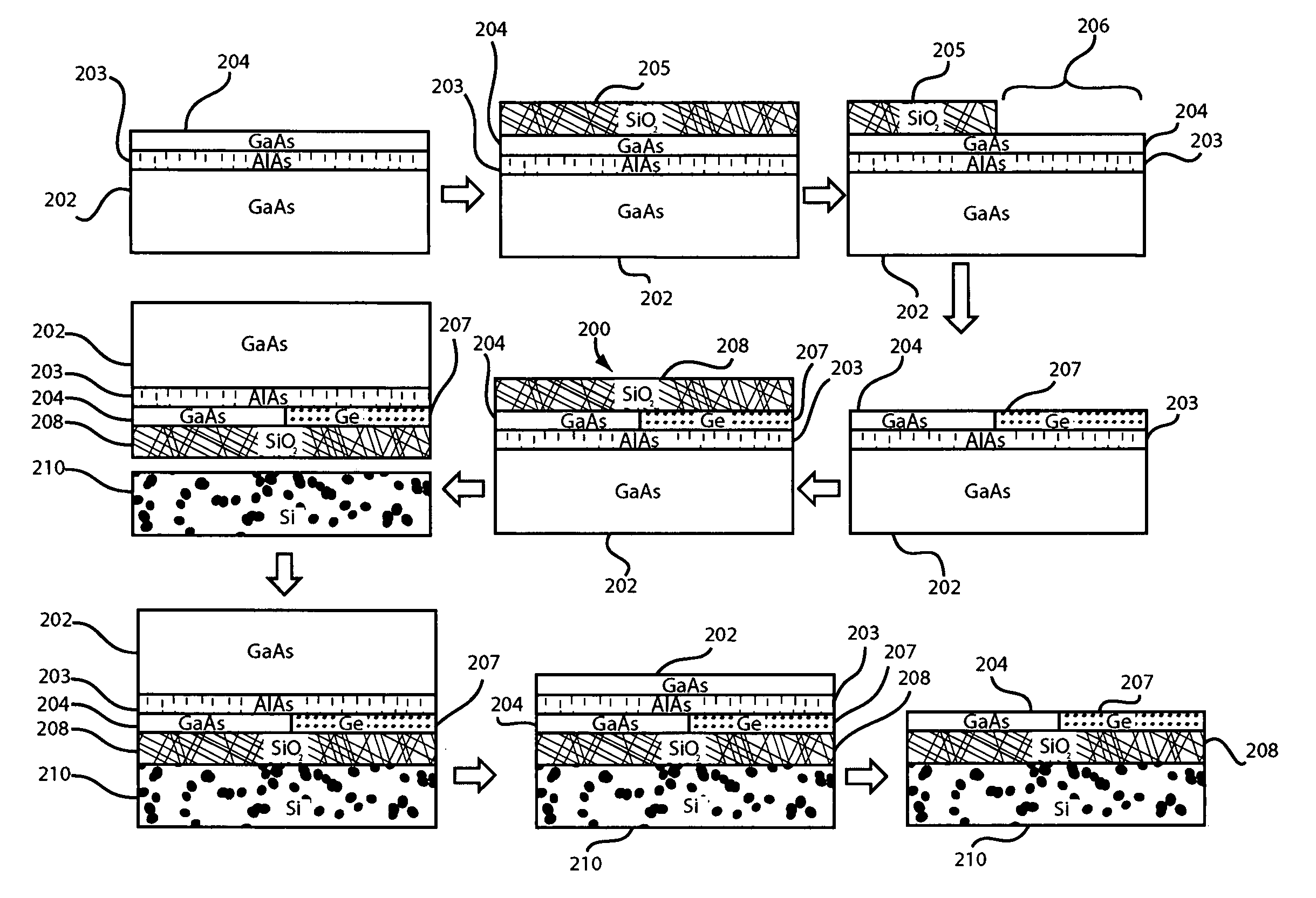
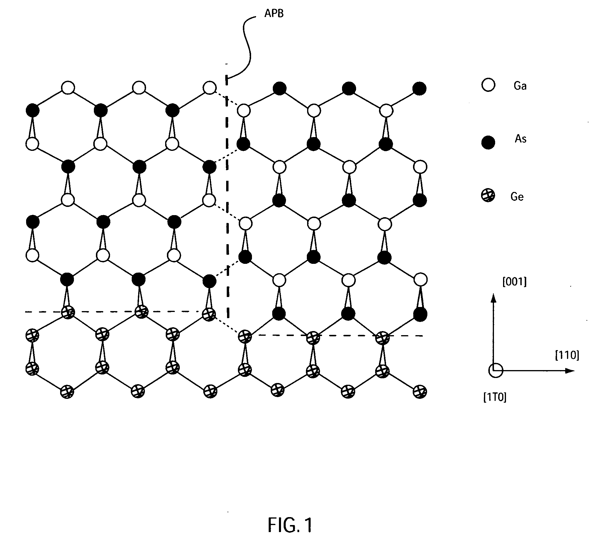
[0021] The present disclosure describes exemplary embodiments for methods and devices, which combine compound and elemental semiconductors onto a silicon (Si) substrate in such a way as to avoid the problem of anti-phase domains in the compound semiconducting material.

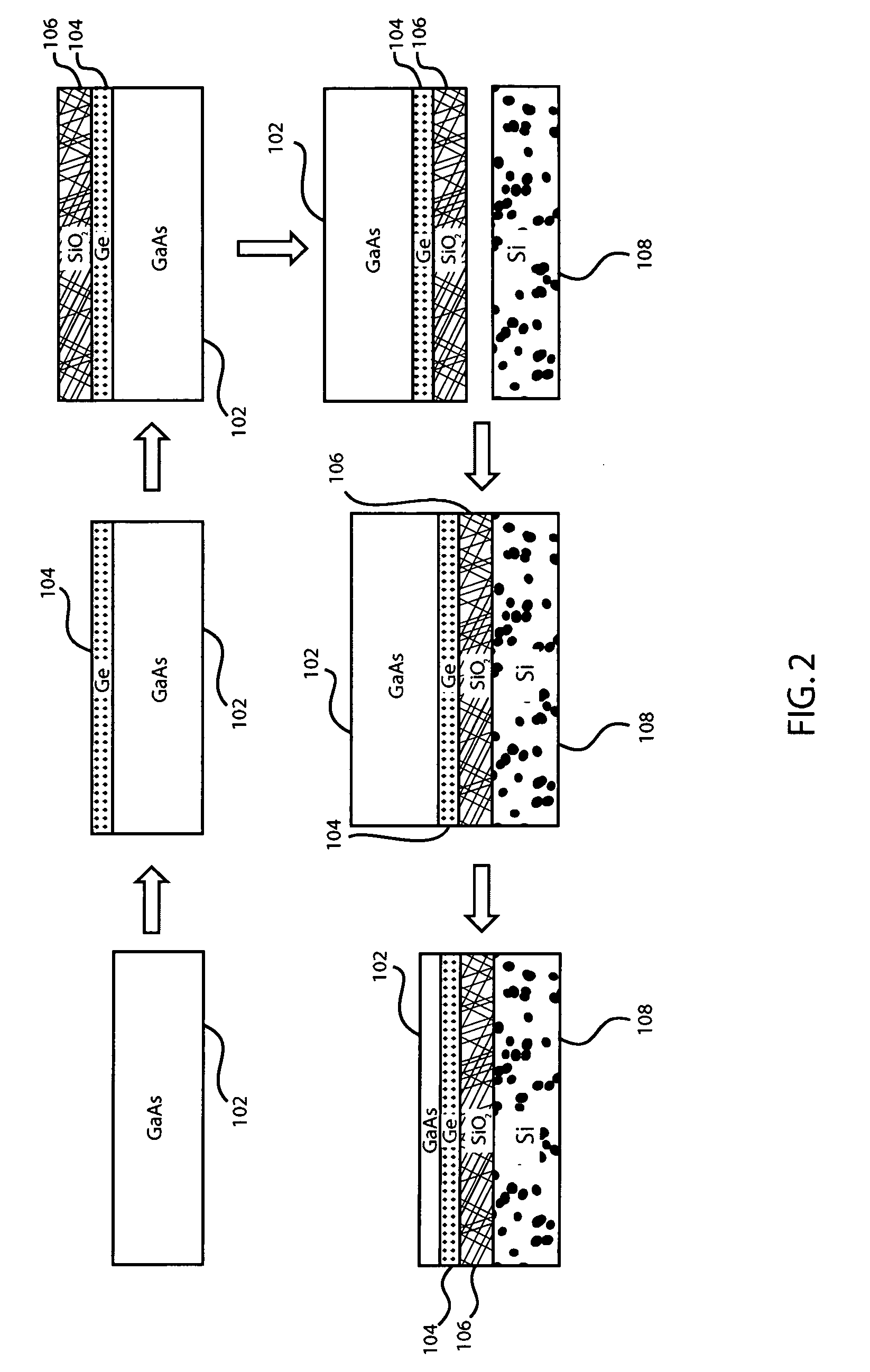
[0022] The one concept is to epitaxially grow an elemental semiconductor on a single-crystal compound semiconductor substrate and then use wafer bonding to transfer the combined compound and elemental semiconductor layer structure onto a Si substrate. This methodology solves the problem of anti-phase domains, because it avoids altogether compound semiconductor growth on an elemental semiconductor.

[0023] This method also creates high-quality films for both the compound and elemental semiconductors because bulk compound semiconductor crystals have low defect densities relative to layers produced by direct growth or compositional growth on Si.

[0024] The teachings of this disclosure could apply to any compound / elemental...


PUM


Abstract

A method for fabricating a semiconductor substrate includes epitaxially growing an elemental semiconductor layer on a compound semiconductor substrate. An insulating layer is deposited on top of the elemental semiconductor layer, so as to form a first substrate. The first substrate is wafer bonded onto a monocrystalline Si substrate, such that the insulating layer bonds with the monocrystalline Si substrate. A semiconductor device includes a monocrystalline substrate, and a dielectric layer formed on the monocrystalline substrate. A semiconductor compound is formed on the dielectric layer and an elemental semiconductor material formed in proximity of the semiconductor compound and lattice-matched to the semiconductor compound.

Description

BACKGROUND [0001] 1. Technical Field [0002] Exemplary embodiments described herein relate to semiconductors and, more particularly, to integrated compound and elemental semiconductor substrates and devices. [0003] 2. Description of the Related Art [0004] Compound semiconductors, particularly III-V semiconductors, are of interest for advanced complementary metal oxide semiconductor (CMOS) technology, due to their superior transport properties compared to silicon (Si). However, the superior transport only applies to electrons. In III-Vs, the hole mobility is only comparable or even degraded compared to elemental semiconductors, such as Si and Ge. [0005] One method for combining III-V and group-IV materials is described by G. B. Gao and H. H. Hoang in U.S. Pat. No. 6,563,143, wherein a method of combining GaAs and Ge, for NFETs and PFETs, respectively, has been proposed. The combination of materials is particularly attractive because GaAs and Ge are lattice matched, and Ge has the high...

Claims


Application Information

Patent Timeline
Patent Type & Authority Applications(United States)
IPC IPC(8): H01L21/30H01L21/46
CPCH01L21/76254H01L21/76256H01L21/823807H01L21/8258H01L21/84H01L27/1203H01L21/02002
Inventor KOESTER, STEVEN JOHNSADANA, DEVENDRA KUMARSHAHIDI, GHAVAM G.
Owner ALSEPHINA INNOVATIONS INC
Why Eureka
Try Eureka