Substrate before insulation, method of manufacturing substrate, method of manufacturing surface acoustic wave transducer, surface acoustic wave device, and electronic equipment
a technology of substrate and insulating layer, which is applied in the direction of instrumentation, circuit masks, photomechanical equipment, etc., can solve the problems of insufficient resist thickness, insufficient manufacturing cost, and fluctuation of frequency and instability of resonance characteristics, so as to shorten the process of manufacturing substrate, easy to remove protection film, and simplify the effect of the instrument manufacturing substra
- Summary
- Abstract
- Description
- Claims
- Application Information
AI Technical Summary
Benefits of technology
Problems solved by technology
Method used
Image
Examples
modification 1
[0112] Modification 1
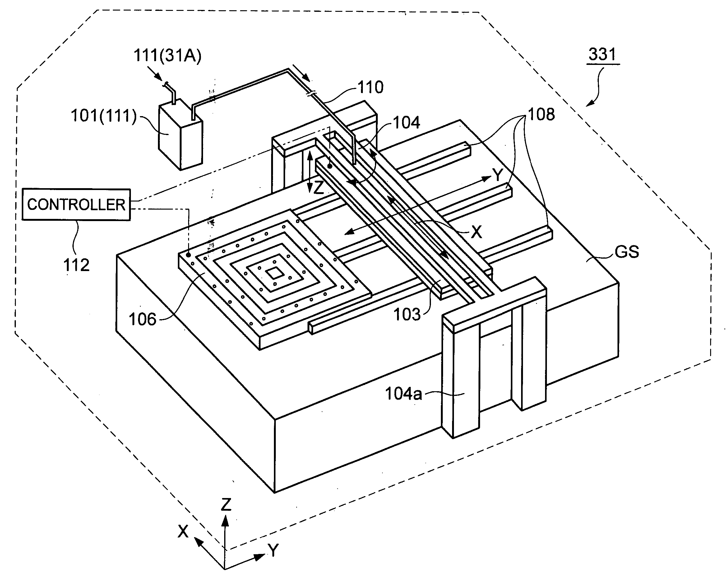
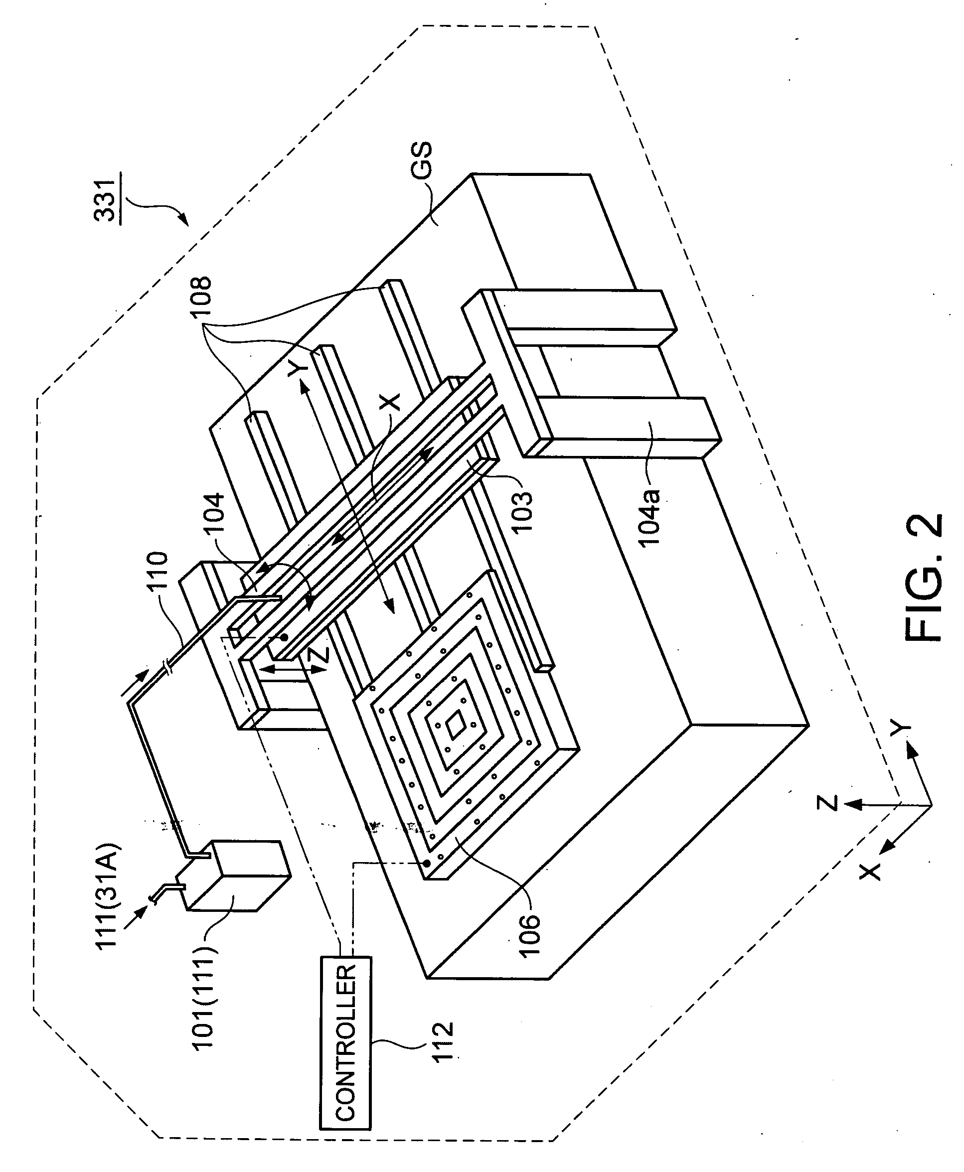
[0113] The above mentioned embodiment includes the process of heating the base 11 by the heater 320 for forming the protection layer 31 which is higher than the thickness of the partition wall 33 and the process of giving the first protection material 31A to the surface of the base 11 by using the droplet-discharging device 331. But, instead of these processes, the first protection material 31A in which the boiling temperature of the solvent is more than 170° C. and under 250° C. may be discharged to the surface of the base by using the droplet-discharging device 331. This is a modification where the ratio a / b can be increased by increasing the boiling temperature of the solvent in the first protection material 31A more than increasing the temperature of the base 11. According to the inventor's experiment, when the boiling temperature of the solvent in the first protection material 31A is more than 170° C. and under 250° C. without heating the base 11, the prote...
modification 2
[0116] Modification 2
[0117] In the above embodiment, the first protection layer 31 included in the protection film 30 comprises the circumferential partition wall 33 and the ground film 34 which is integrally formed with the circumferential partition wall 33. But, the ground film 34 may be omitted. FIGS. 15A and 15B show this modification. In FIGS. 15A and 15B, the first protection layer 31 only comprises the circumferential partition wall 33, which is placed outer circumferential area of the protection region and the second protection layer 32 is placed so as to be embedded covering over the region surrounded by the partition wall. The protection film 30 comprises the first protection layer 31 and the second protection layer 32 and is placed on a surface of a part of the base 11. FIG. 15B is an enlarged view of the conductive pad 21 of the base 11 and FIG. 15A is a cross section when the base 11 is cut along the line E-E in FIG. 15B. Thus, in the protection film 30 including the fi...
modification 3
[0120] Modification 3
[0121] In the above mentioned embodiment, anode oxidization process was used for insulating the surface of the aluminum thin film, but any other methods may be used if a layer for insulating the surface of the base 11 can be formed. For example, the thermal oxidization may be used in which the base 11 is put into a processing unit filled with a gas such as oxygen and heated. Thus, the substrate having the insulation layer 40 only in the desired area among the surface of the base may be manufactured by this method for manufacturing the base including such insulation process.
PUM
 Abstract
Description
Claims
Application Information


