Method for producing a semiconductor wafer

a technology of semiconductor wafers and semiconductor layers, applied in the direction of crystal growth process, polycrystalline material growth, chemically reactive gases, etc., can solve the problems of poor yield, high substrate cost, bubbles, cracks, etc., and achieve the effect of preventing dislocation, excess thickness, and preventing surface roughness

Inactive Publication Date: 2006-08-24
SHIN-ETSU HANDOTAI CO LTD
View PDF23 Cites 6 Cited by
  • Summary
  • Abstract
  • Description
  • Claims
  • Application Information

AI Technical Summary

Benefits of technology

[0013] If an ion-implanted layer for delamination is formed inside the silicon single crystal wafer by implanting at least one kind of hydrogen ion and rare gas ion through the strained Si layer with the increased thickness and a surface of the strained Si layer with the increased thickness of the silicon single crystal wafer as a bond wafer and a surface of a base wafer are closely bonded directly or through an insulator film, this has a sufficient thickness for device production, and there is no surface-roughness by crosshatch in the strained Si layer and therefore void defects are not generated when they are bonded. And thereafter, if delamination is performed at the ion-implanted layer for delamination and the strained Si layer with the increased thickness is exposed by removing the most surficial Si layer and the Si1-XGeX layer transferred to the side of the base wafer by the delamination, dislocation and surface-roughness are prevented, there can be produced a semiconductor wafer having a SSOI structure formed with the strained Si layer that has sufficient strain and has a thickness which can apply to device designs of various specifics.
[0014] Moreover, the present invention provides a method for producing a semiconductor wafer comprising at least steps of, forming a Si1-XGeX layer (0<X<1) with a critical film-thickness at a deposition temperature of the layer or thinner on a surface of a silicon single crystal wafer and then forming a Si layer with a critical film-thickness at a temperature of a later relaxing heat-treatment or thinner thereon, forming an ion-implanted layer for relaxation inside the silicon single crystal wafer by implanting at least one kind of hydrogen ion, rare gas ion, and Si ion through the Si layer, thereafter performing the relaxing heat-treatment, thereby to make the Si1-XGeX layer lattice-relaxed and to form a strained Si layer by introducing lattice strain in the Si layer, thereafter forming an ion-implanted layer for delamination inside the silicon single crystal wafer by implanting at least one kind of hydrogen ion and rare gas ion through the strained Si layer, closely bonding a surface of the strained Si layer of the silicon single crystal wafer as a bond wafer and a surface of a base wafer directly or through an insulator film, thereafter performing delamination at the ion-implanted layer for delamination, exposing the strained Si layer by removing the most surficial Si layer and the Si1-XGeX layer transferred to the side of the base wafer by the delamination, and thereafter depositing Si on a surface of the strained Si layer, and thereby to increase a thickness of the strained Si layer.
[0015] Also, in the case that after a strained Si layer having no misfit dislocation is formed by formation of an ion-implanted layer for relaxation and relaxing heat-treatment, each of steps such as forming a ion-implanted layer for delamination, bonding of wafers, delaminating, and exposing the strained Si layer is performed and thereafter a step of depositing Si to increase a thickness of the strained Si layer is performed as described above, void defects are not generated even when they are bonded, dislocation and surface-roughness are prevented, and there can be produced a semiconductor wafer having a SSOI structure formed with the strained Si layer that has sufficient strain and has a thickness which can apply to device designs of various specifics.
[0021] If the thickness of the Si layer with the critical film-thickness or thinner to be formed is from 3 nm to 10 nm as described above, misfit dislocation can be surely prevented from being generated in relaxing heat-treatment, and the thickness can become so sufficient that the layer is not feared to be perfectly removed by etching action in cleaning.
[0028] According to the present invention, if a Si1-XGeX layer with a critical film-thickness at a deposition temperature of the layer or thinner is formed on a surface of a silicon single crystal wafer and then a Si layer with a critical film-thickness at a temperature of later relaxing heat-treatment or thinner is formed thereon and an ion-implanted layer for relaxation is formed inside the silicon single crystal wafer by implanting hydrogen ion and such through the Si layer and thereafter the relaxing heat-treatment is performed and thereby to make the Si1-XGeX layer lattice-relaxed and to form a strained Si layer by introducing lattice strain in the Si layer as described above, misfit dislocation is not generated in the strained Si layer in the relaxing heat-treatment, generation of threading-dislocation can be suppressed, surface-roughness by generation of crosshatch can be suppressed, and a favorable strained Si layer can be formed. And thereafter, if Si is deposited on a surface of the strained Si layer and thereby to increase a thickness of the strained Si layer, dislocation and surface-roughness can be suppressed and there can be produced a semiconductor wafer having a strained Si layer that has sufficient strain corresponding to lattice relaxation of the Si1-XGeX layer and has a thickness which can apply to device designs of various specifics.

Problems solved by technology

However, in the case that a SSOI wafer is produced by this method, the bulk SiGe substrate as described above requires a thick Graded SiGe layer having several micrometers, therefore throughput is bad and the substrate becomes very expensive.
In this case, bubble, crack, crystal defect and such are formed in the ion-implanted layer.

Method used


Image

  • Method for producing a semiconductor wafer
  • Method for producing a semiconductor wafer

Examples


experiment 1

[0032] Accordingly, the present inventors produced wafers (samples 1 to 3) which were formed with a Si1-XGeX layer and a strained Si layer on a silicon single crystal wafer using the method described above. For investigating the properties thereof, a relaxation rate of each of the Si1-XGeX layers were measured by a micro-Raman measurement method. The measurement was performed using RS-3000 manufactured by HORIBA Ltd., an apparatus using a micro-Raman method. Here, a relaxation rate is the amount relatively represented by a degree of lattice relaxation, where the rate is 0% in the case that a lattice constant of the Si1-XGeX layers is the same with that of Si and the rate is 100% in the case of the inherent lattice constant determined by a Ge concentration. Production conditions of the wafers and measurement results is shown in Table 1. In addition, in each of the samples, the Si1-XGeX layer was set to be X=0.2, the dose amount of hydrogen ions was set to be 3.0×10¹⁶ / cm2, a depositio...

experiment 2

[0035] Next, for investigating the relation of a thickness of a Si layer to which strain is introduced and a strain amount, by the same method with Experiment 1, wafers each having a Si layer with a different thickness were produced. As a bond wafer, each of the wafers was bonded to a base wafer and thereby there was produced SSOI wafers (Samples 4 to 6) as the same manner with the conventional method described above. A strain amount of the strained Si layer was measured by a micro-Raman measurement method. Here, a strain amount is the amount represented by how much a lattice constant of a strained Si layer is expanded or shrank against the lattice constant of Si. In the present specification, in the case of expanding the amount is a positive value. The results are shown in Table 2. In addition, in each of the samples, a thickness of the Si1-XGeX layer was 100 nm, the dose amount of hydrogen ions was set to be 3.0×10¹⁶ / cm2, and relaxing heat-treatment was performed at 900° C. for 7 ...

examples

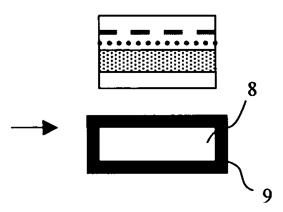
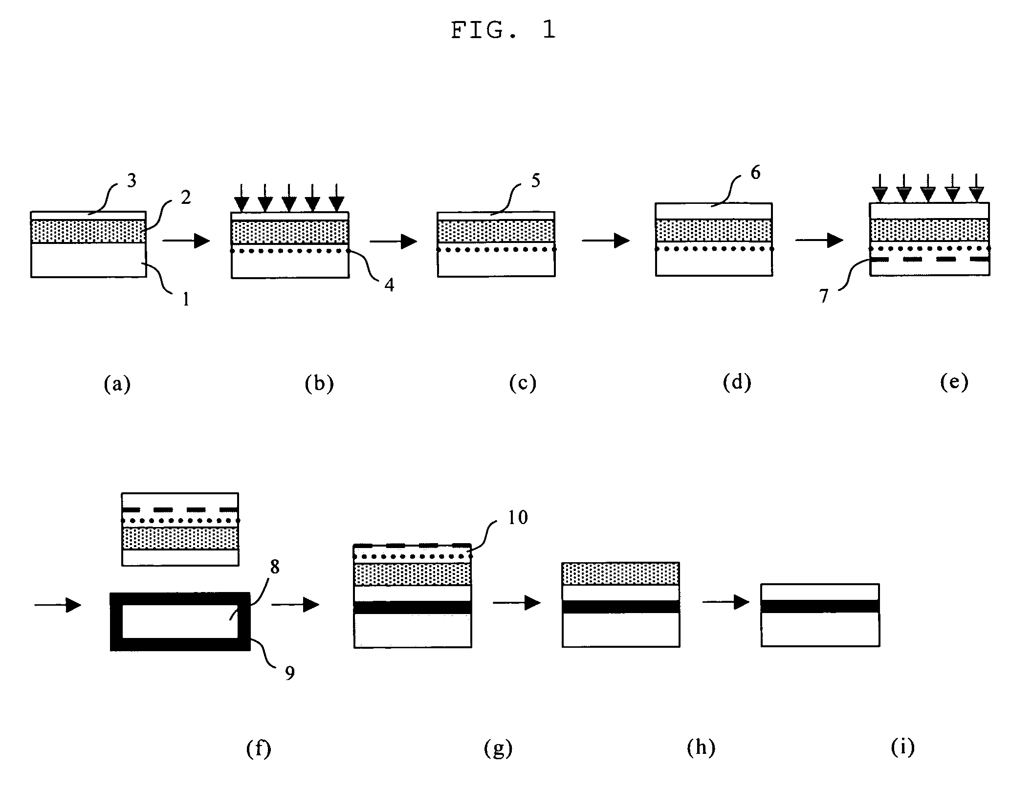
[0063] Hereinafter, examples and comparative examples according to the present invention will be explained concretely. However, the present invention is not limited thereto. (Example 1, 2, Comparative Example 1, 2) According to the steps shown in FIG. 1, SSOI wafers were produced (Example 1, 2). Moreover, SSOI wafers were produced according to the steps as shown in FIG. 1 except for not performing a step of increasing a thickness of the strained Si layer (Comparative Example 1, 2). And, strain amounts of the strained Si layers of these SSOI wafers were measured. In addition, the measurements of the strain amounts were performed by using RS-3000 manufactured by HORIBA, Ltd., an apparatus using a micro-Raman method. Moreover, in Examples 1, 2, and Comparative Example 1, a thickness of the Si layer formed on the Si1-XGeX layer is set to be 10 nm, a critical film-thickness at a temperature of the relaxing heat-treatment (900° C.) or thinner, and in Comparative Example 2, 25 nm, the crit...


PUM

PropertyMeasurementUnit
thicknessaaaaaaaaaa
temperatureaaaaaaaaaa

Abstract

The present invention provides a method for producing a semiconductor wafer comprising at least steps of, forming a Si1-XGeX layer (0<X<1) with a critical film-thickness at a deposition temperature of the layer or thinner on a surface of a silicon single crystal wafer and then forming a Si layer with a critical film-thickness at a temperature of later relaxing heat-treatment or thinner thereon, forming an ion-implanted layer for relaxation inside the silicon single crystal wafer by implanting at least one kind of hydrogen ion, rare gas ion, and Si ion through the Si layer, thereafter performing the relaxing heat-treatment, thereby to make the Si1-XGeX layer lattice-relaxed and to form a strained Si layer by introducing lattice strain in the Si layer, thereafter depositing Si on a surface of the strained Si layer, and thereby to increase a thickness of the strained Si layer. Thereby, there is provided a method for producing a semiconductor wafer formed with a strained Si layer in which misfit dislocation is not generated and the layer has sufficient strain and has a thickness which can apply to device designs of various specifics.

Description

BACKGROUND OF THE INVENTION [0001] 1. Field of the Invention [0002] The present invention relates to a method for producing a semiconductor wafer in which a strained Si layer is formed, for example, on an insulator. [0003] 2. Description of the Related Art [0004] In recent years, in order to meet demands for high-speed semiconductor devices, on a Si (silicon) single crystal wafer, a Si1-XGeX layer (0<X<1, hereinafter occasionally described as a SiGe layer simply) and a Si layer are epitaxial-grown in order. There has been proposed semiconductor devices, such as a high-speed MOSFET (Metal-Oxide-Semiconductor Field Effect Transistor), in which the Si layer is used in a channel region. [0005] In this case, because a Si1-XGeX crystal is larger than a Si crystal in a lattice constant, tensile strain is caused in a Si crystal epitaxial-grown on a Si1-XGeX layer (hereinafter, the Si layer in which strain is caused is referred to as a strained Si layer). An energy band structure of a ...

Claims


Application Information

Patent Timeline
Patent Type & Authority Applications(United States)
IPC IPC(8): C30B23/00C30B25/00C30B28/12C30B28/14
CPCC30B29/06C30B29/52C30B31/22
Inventor AGA, HIROJINOTO, NOBUHIKOMITANI, KIYOSHI
Owner SHIN-ETSU HANDOTAI CO LTD
Why Eureka
Try Eureka