Sensor for detecting a target substance in a fluid
- Summary
- Abstract
- Description
- Claims
- Application Information
AI Technical Summary
Problems solved by technology
Method used
Image

Examples
example 1
[0301] An example of a sensor device is shown below which employs the aforementioned photonic crystal in combination with a light source as the light-projecting means, and detector as the means for detecting the emitted light.
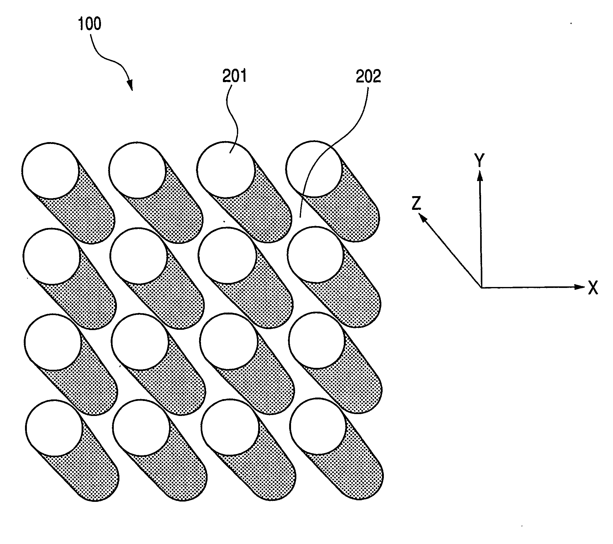
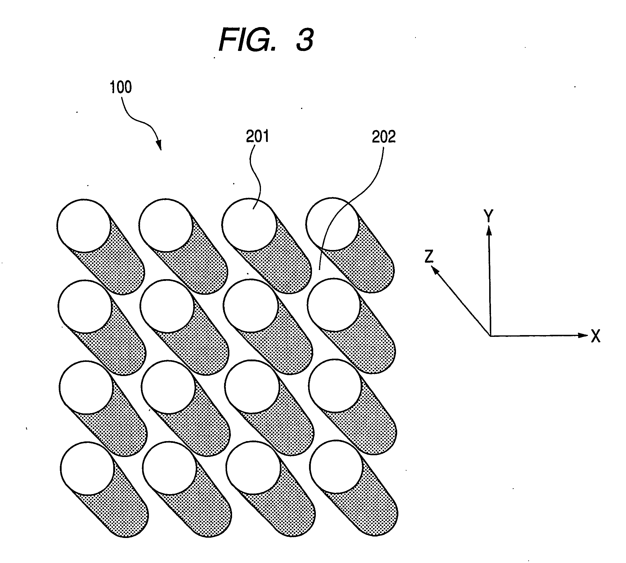
[0302]FIG. 38 shows a first example of the sensor of the present invention. The numeral 3800 denotes a main body package of a biosensor, and the numeral 100 denotes a photonic crystal structure. The photonic crystal structure in FIG. 38 has holes 202 arranged periodically in a solid. A test sample liquid is passed through the holes. A trapping substance is held on the surface of the holes. A light beam from light source 402 of a laser or the like is collimated and is projected to photonic crystal structure 100. The light having been transmitted through the photonic crystal is introduced to signal light detector 404. The change in photonic band gap energy is detected by signal light detector 404. The presence or absence of the target substance is detected from ...
example 2
[0307]FIG. 39 shows a second example of the sensor of the present invention. Biosensor unit 3900 has photonic crystal 3901 containing a reactive substance. External units 3902 contain light-emitting means 402 and signal light-detecting means 404. Biosensor 3900 having the photonic crystal is connected thereto.
[0308] The sensor of this example is equipped with an aligning mechanism which serves to introduce the light beam generated by the light source in the external unit into the photonic crystal and serves to introduce the light beam emitted from the sensor unit into a light detecting means in the external unit. The aligning mechanism specifically may be a simple one having a protrusion and a depression for coupling. An example is shown in FIG. 39 which has protrusion 3905 provided on biosensor unit 3900 and a depression 3906 provided on external unit 3902. Preferably the aligning mechanism has further a function for adjusting the light introduction position on the photonic crysta...
example 3
[0310]FIGS. 40 and 41 show an example of the sensor of the present invention. FIG. 40 is a perspective view of the sensor. FIG. 41 is a sectional view taken at a plane 41-41 parallel to the ZX plane including optical waveguide 4007. SOI (Silicon on Insulator) substrate 4001 is a thin film constituted of base plate 4002, insulating layer 4003 of about 1 μm thick, and SOI layer 4004 of about 200 nm. In SOI layer 4004, there are formed grooves 4006 of about 1 μm wide to provide two optical waveguides 4007 therebetween, and holes of about 110 nm in radius bored in the layer thickness direction arranged in a two-dimensional triangle lattice at a lattice constant of about 400 nm in the region of 100 μm×100 μm between the two optical waveguide 4007 by electron ray lithography and dry etching, or a like process. The periodic structure having plural holes arranged periodically functions as a photonic crystal. The insulating layer is also called a BOX layer (Barried Oxide Layer). A part of in...
PUM
 Abstract
Description
Claims
Application Information
 - Generate Ideas
- Intellectual Property
- Life Sciences
- Materials
- Tech Scout
- Unparalleled Data Quality
- Higher Quality Content
- 60% Fewer Hallucinations
Browse by: Latest US Patents, China's latest patents, Technical Efficacy Thesaurus, Application Domain, Technology Topic, Popular Technical Reports.
© 2025 PatSnap. All rights reserved.Legal|Privacy policy|Modern Slavery Act Transparency Statement|Sitemap|About US| Contact US: help@patsnap.com