High-luminescence silicon electroluminescence device

a high-luminescence, silicon electroluminescence technology, applied in the direction of semiconductor/solid-state device details, final product manufacturing, coatings, etc., can solve the problems of bulk silicon being a highly inefficient light emitter, unsuitable for optoelectronic applications, and poor light generation efficiency, etc., to achieve the effect of increasing the refractive index of the sro film

Inactive Publication Date: 2006-08-24
SHARP KK
View PDF4 Cites 31 Cited by
  • Summary
  • Abstract
  • Description
  • Claims
  • Application Information

AI Technical Summary

Benefits of technology

[0015] SRO thin-films with a high density of correctly-sized Si nano-particles, which may alternately be understood as Si size distribution, can be made by PECVD and sputtering processes. The best quality of Si nanocrystal / SiO2 interface comes from thermal oxidation. The high temperature enhances the silicon diffusion process, and helps grow the Si nanocrystals, making the film dense with Si nanocrystals. At the same time, the thermal oxidation balances the nano-Si particle size, while improving the SiO2 / Si nanocrystal interface quality. The strong oxidants, the smaller-molecule carrier gas, and small porosity of the as-deposited SRO thin-films enhance the homogeneous oxidation of nano-Si particles throughout the film. Using these processes, a high-luminance SRO film can be obtained.
[0018] In another aspect, the method comprises thermal annealing the SRO film in an atmosphere void of oxygen, prior to post-annealing the SRO film in an oxygen atmosphere. Typically, thermal annealing the SRO film in an atmosphere void of oxygen increases the refractive index of the SRO film, forms Si nanocrystals in the SRO film, and densifies the SRO film.

Problems solved by technology

For silicon devices, the light generation efficiency is known to be poor and the photon energy is predominantly around 2 eV.
However, these devices are fabricated on materials that are typically not compatible with silicon, for example type III-V materials such as InGaN, AlGaAs, GaAsP, GaN, and GaP.
Silicon has conventionally been considered unsuitable for optoelectronic applications, due to the indirect nature of its energy band gap.
Bulk silicon is indeed a highly inefficient light emitter.
However, these SRSO materials exhibit low quantum efficiency and have a stability problem, which reduces the PL intensity height over time, and limits their application to EL devices.
However, state-of-the-art implantation processes have not been able to distribute the dopant uniformly, which lowers the light emitting efficiency and increases costs.
At the same time, there has been no interface engineering sufficient to support the use of such a dopant.
Using the Si / SiO2 superlattice structure to control crystal size results in a slow, high-temperature deposition process that cannot simultaneously control both the Si particle size and the quality Si nanocrystal / SiO2 interface.
The device efficiency is very low, which limits the device applications.

Method used


Image

  • High-luminescence silicon electroluminescence device
  • High-luminescence silicon electroluminescence device
  • High-luminescence silicon electroluminescence device

Examples


Embodiment Construction

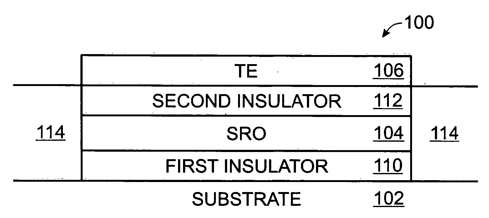
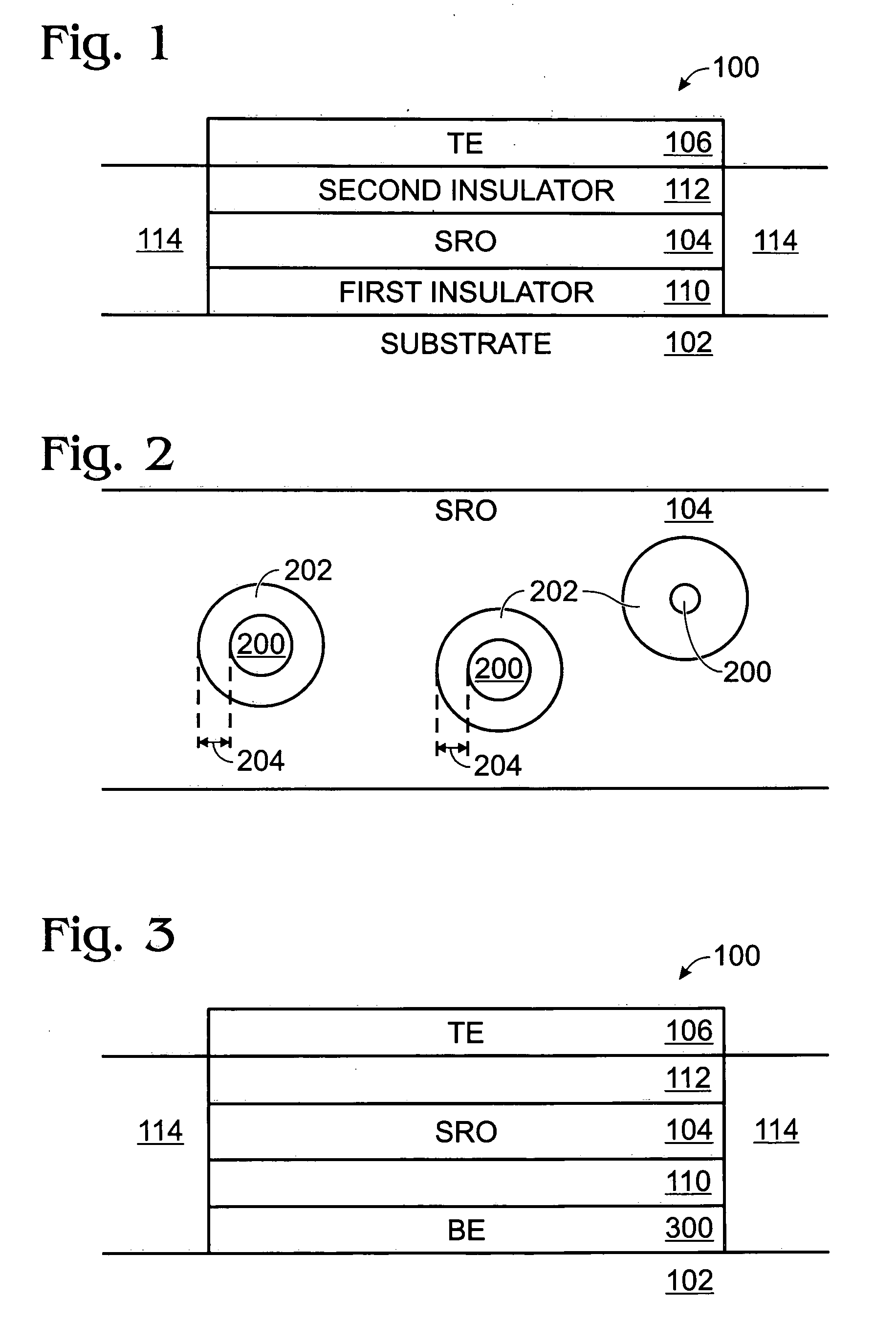
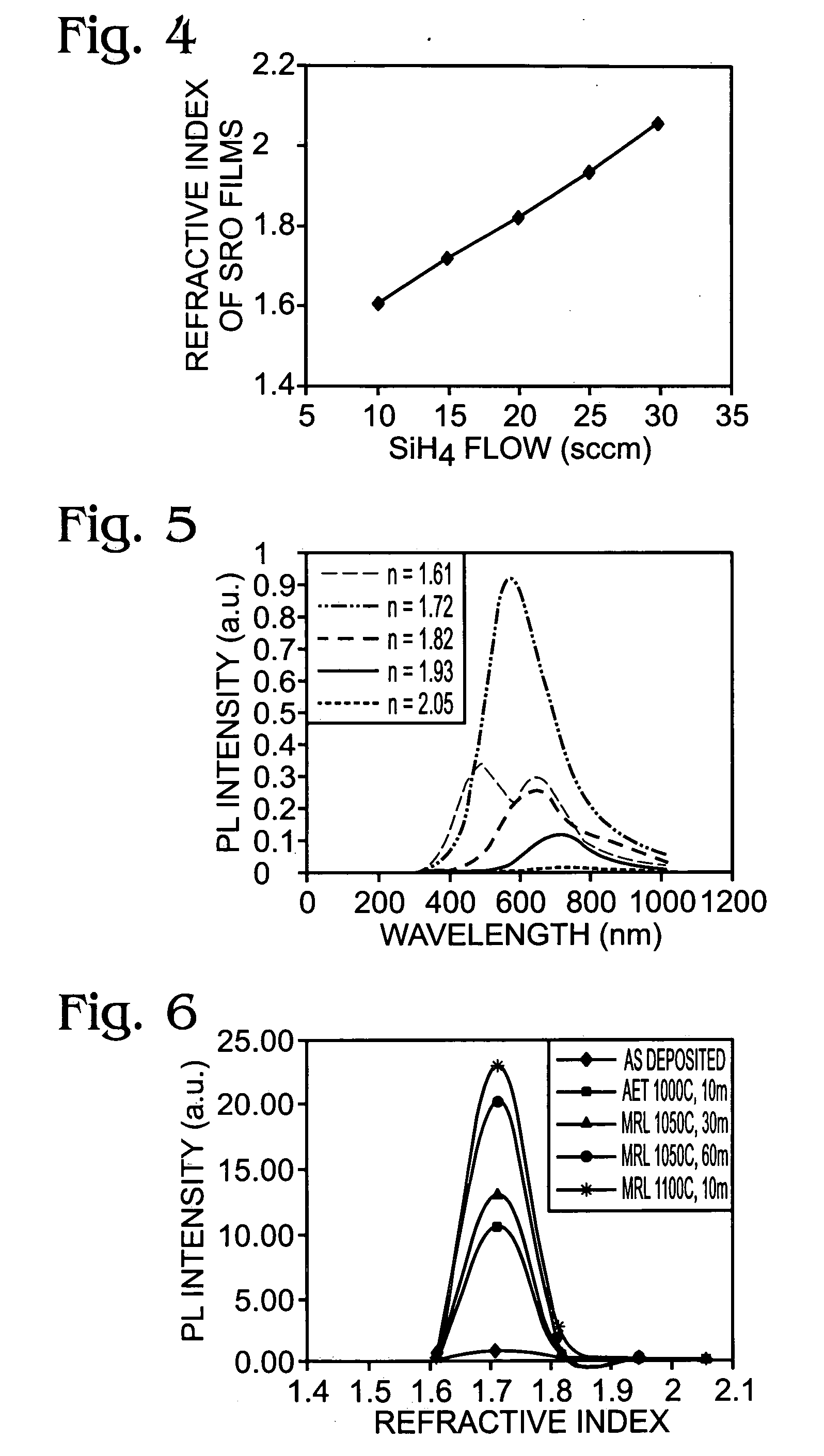
[0035]FIG. 1 is a partial cross-sectional view of a high-luminescence silicon (Si) electroluminescence (EL) device. In its simplest form, the EL device 100 comprises a substrate 102 and a silicon-rich oxide (SRO) film 104 overlying the substrate 102. The SRO film 104 has a refractive index in the range of 1.5 to 2.1, and a porosity in the range of 5 to 20%. A top electrode (TE) 106 overlies the SRO film 104. The index of refraction relates to the bending of light as it passes through a transparent or semi-transparent medium. Alternately stated, the index of refraction is a ratio, representing the difference in the propagation of light through a particular medium, as opposed to air. Porosity is the proportion of the non-solid volume to the total volume of material, and is defined by the ratio: ϕ=VpVm

[0036] where Vp is the non-solid volume (pores) and Vm is the total volume of material, including the solid and non-solid parts. It is common to express porosity as a percentage.

[0037]F...


PUM

PropertyMeasurementUnit
porosityaaaaaaaaaa
refractive indexaaaaaaaaaa
thicknessaaaaaaaaaa

Abstract

A method for forming a high-luminescence Si electroluminescence (EL) phosphor is provided, with an EL device made from the Si phosphor. The method comprises: depositing a silicon-rich oxide (SRO) film, with Si nanocrystals, having a refractive index in the range of 1.5 to 2.1, and a porosity in the range of 5 to 20%; and, post-annealing the SRO film in an oxygen atmosphere. DC-sputtering or PECVD processes can be used to deposit the SRO film. In one aspect the method further comprises: HF buffered oxide etching (BOE) the SRO film; and, re-oxidizing the SRO film, to form a SiO2 layer around the Si nanocrystals in the SRO film. In one aspect, the SRO film is re-oxidized by annealing in an oxygen atmosphere. In this manner, a layer of SiO2 is formed around the Si nanocrystals having a thickness in the range of 1 to 5 nanometers (nm).

Description

BACKGROUND OF THE INVENTION [0001] 1. Field of the Invention [0002] This invention generally relates to integrated circuit (IC) fabrication and, more particularly, to an electroluminescence (EL) device with a silicon-rich oxide (SRO) film having a refractive index of about 1.72, to optimize photoluminescence (PL). [0003] 2. Description of the Related Art [0004] The generation of light from semiconductor devices is possible, regardless of whether the semiconductor material forms a direct or indirect bandgap. High field reverse biased p-n junctions create large hot carrier populations that recombine with the release of photons. For silicon devices, the light generation efficiency is known to be poor and the photon energy is predominantly around 2 eV. The conversion of electrical energy to optical photonic energy is called electroluminescence (EL). Efficient EL devices have been made that can operate with small electrical signals, at room temperature. However, these devices are fabrica...

Claims


Application Information

Patent Timeline
Patent Type & Authority Applications(United States)
IPC IPC(8): H01L21/00
CPCH01L31/03046Y02E10/544Y02P70/50
Inventor LI, TINGKAIJOSHI, POORAN CHANDRAGAO, WEIONO, YOSHIHSU, SHENG TENG
Owner SHARP KK
Why Eureka
Try Eureka