Communication semiconductor integrated circuit, a wireless communication apparatus, and a loop gain calibration method

a technology of communication semiconductor and integrated circuit, which is applied in the direction of gain control, phase-modulated carrier system, digital transmission, etc., can solve the problems of difficulty in meeting specifications, precision of modulation, and degree of noise suppression, so as to reduce variation, open loop, and calculate the variation of amplifier loop gain

Inactive Publication Date: 2006-08-24
TAKANO RYOICHI +4
View PDF25 Cites 59 Cited by
  • Summary
  • Abstract
  • Description
  • Claims
  • Application Information

AI Technical Summary

Benefits of technology

[0010] In addition, in two feedback loops, the loop gain particularly of the amplifier control loop varies due to dispersion or variation in characteristics of constituent components in production and hence stability of the loop decreases, and hence it is difficult to obtain a desired output level in a specified or predetermined period of time. It has been also detected that the system of the polar loop has a problem that when an output control operation is conducted for the amplitude modulation in the amplitude control loop, the gain of the amplitude control loop changes to reduce a phase margin and hence stability of the loop is lowered.
[0011] It is therefore an object of the present invention to improve the modulating precision of a transmission waveform and the spectral re-growth and to sufficiently suppress noise in a receiving frequency bandwidth in a wireless communication apparatus such as a portable telephone having a function to conduct phase modulation and amplitude modulation.
[0012] Another object of the present invention is to provide a reliable wireless communication apparatus which prevents degradation in stability of a loop due to variation in a loop gain caused by dispersion in characteristics of constituent components in production.
[0013] Still another object of the present invention is to provide a reliable wireless communication apparatus which prevents, when an output control operation is conducted for amplitude modulation, degradation in stability of a loop due to decrease in a phase margin caused by variation in an amplitude control loop gain.
[0015] In a wireless communication apparatus of polar loop type having a phase control loop to control a phase of a carrier wave or signal outputted from a transmission oscillator and an amplitude control loop to control amplitude of a transmission output signal outputted from a power amplifier circuit, there are disposed, on a forward path from an amplifier detector circuit to a power amplifier circuit which constitute the amplifier control loop, a variable gain amplifier circuit and a switching unit capable of conducting a change-over of a characteristic of a loop filter for a frequency bandwidth of the amplitude control loop to a degree lower than a degree of the filter in an ordinary operation. While the system is being operated in a state in which the loop filter characteristic is changed to the lower-degree filter characteristic, the output from the power amplifier is measured in this state to calculate variation in the gain of the amplifier loop. According to a result of the calculation, there is obtained data to calibrate or to correct the gain characteristic of the variable gain amplifier circuit with respect to an output control signal in order to reduce the variation. The correction or corrective data thus obtained is stored in a nonvolatile memory in a baseband large scale integration (LSI) chip. Resultantly, by changing the loop filter characteristic to the lower-degree filter characteristic, the measurement can be conducted when the amplitude control loop is in a more stable state. Additionally, by correcting the gain characteristic of the variable gain amplifier circuit with respect to an output control signal according to the correction data beforehand measured and stored in the nonvolatile memory, it is possible to calibrate or to correct the variation in the gain of the amplitude control loop caused by the dispersion in characteristics of constituent components in production.
[0016] According to the present invention, there is provided a wireless communication apparatus of polar loop type having a phase control loop to control a phase of a carrier wave outputted from a transmission oscillator and an amplitude control loop to control amplitude of a transmission output signal outputted from a power amplifier circuit. A variable gain amplifier circuit is disposed in a feedback path from a transmission output level detector circuit to an amplitude detector circuit which constitute the amplitude control loop. A variable gain amplifier circuit is disposed also in a forward path from the amplitude detector circuit to the power amplifier circuit of the loop. Gains of the variable gain amplifier circuits are controlled in mutually opposing directions and the sum of gain of the power amplifier circuit and gain respectively of the variable gain amplifier circuits is controlled to be fixed regardless of the output control signal. As a result, even when the output power is changed, the open loop gain of the amplitude control loop can be kept fixed. This prevents the degradation of stability of the loop due to the variation or deviation in the loop gain.

Problems solved by technology

As a result, there has been detected a problem that when the 8-PSK modulation is carried out in the polar loop method, it is difficult to satisfy requirements of specifications of, for example, precision of modulation for a transmission waveform (error vector magnitude (EVM)) and a degree of noise suppression.
Specifically, there is a problem in which while the modulating precision is higher and a characteristic called “spectral re-growth” indicating a degree of waveform distortion becomes better when the frequency bandwidth of the amplitude control loop (a frequency range from a central frequency of the transmission carrier wave to a frequency thereof for which an open loop gain is 0 decibel (dB)) is wider, attenuation of the amplitude control loop becomes smaller for a receiving or reception frequency apart from 20 megaherz (MHz) from the central frequency of the transmission carrier wave and a sufficient degree of noise suppression cannot be obtained when the bandwidth is wide.
In addition, in two feedback loops, the loop gain particularly of the amplifier control loop varies due to dispersion or variation in characteristics of constituent components in production and hence stability of the loop decreases, and hence it is difficult to obtain a desired output level in a specified or predetermined period of time.
It has been also detected that the system of the polar loop has a problem that when an output control operation is conducted for the amplitude modulation in the amplitude control loop, the gain of the amplitude control loop changes to reduce a phase margin and hence stability of the loop is lowered.

Method used


Image

  • Communication semiconductor integrated circuit, a wireless communication apparatus, and a loop gain calibration method
  • Communication semiconductor integrated circuit, a wireless communication apparatus, and a loop gain calibration method
  • Communication semiconductor integrated circuit, a wireless communication apparatus, and a loop gain calibration method

Examples


Embodiment Construction

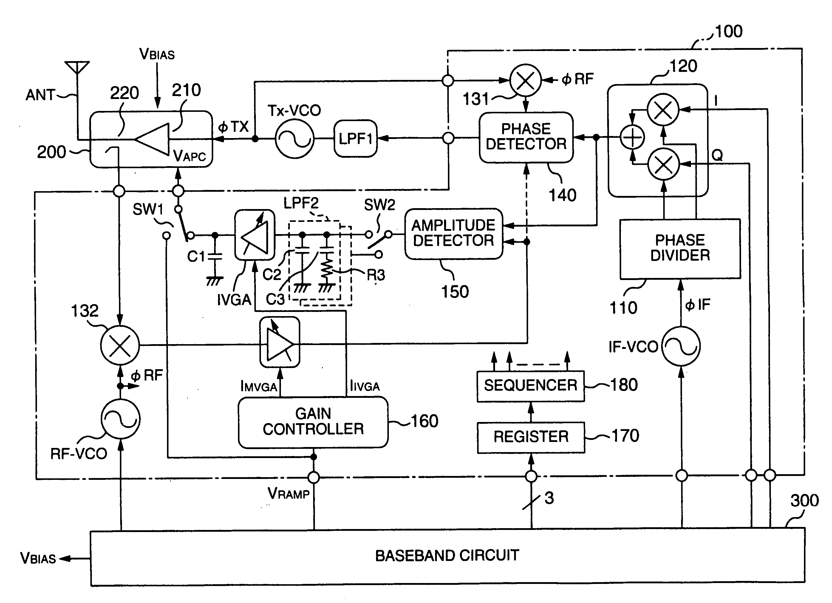
[0041]FIG. 1 shows an outline of a configuration of an embodiment of a transmitting circuit of polar loop type according to the present invention. The configuration of FIG. 1 includes a high-frequency integrated circuit (IC) 100 to conduct GMSK modulation in a GSM system or 8-PSK modulation in an EDGE system, a power module 200 including a high-frequency power amplifier circuit (to be abbreviated as a power amplifier hereinbelow) 210 to conduct communication via an antenna ANT and a coupler 220 to detect transmission power, a baseband circuit 300 which generates an I / Q signal according to transmission data (a baseband signal), a control signal of the radio-frequency IC 100, and a bias voltage VBIAS for the power amplifier 210 in the power module 200, a transmission oscillator TxVCO to generate a phase-modulated transmission signal (carrier wave), and a loop filter LPF1 to limit a bandwidth of a phase control loop.

[0042] The radio-frequency IC 100 is a semiconductor integrated circu...


PUM


Abstract

A polar-loop wireless communication apparatus includes, on a forward path between an amplitude detector and a power amplifier which constitute an amplitude control loop, a variable gain amplifier and a switch to change characteristics of a loop filter to output a frequency bandwidth of the amplitude control loop to an order less than an order for normal operation. The system is operated with the characteristics set to the lower order to measure outputs from the power amplifier to calibrate the output power of the power transmitter, and the register is operated with the characteristics set to the higher order to measure the open loop gain of the amplitude control. According to results of the calculation, data to correct gain characteristics of the variable gain amplifier with respect to an output control signal is stored in a nonvolatile memory of a baseband circuit.

Description

CROSS-REFERENCE TO RELATED APPLICATION [0001] The present application relates to subject matters described in the U.S. patent applications being file based on the United Kingdom Patent Applications No. 0212737.1 filed on May 31, 2002, No. 0212729.8 filed on May 31, 2002, No. 0212723.1 filed on May 31, 2002, No. 0212735.5 filed on May 31, 2002, and No. 0212732.2 filed on May 31, 2002. All of those U.S. applications are assigned to the same assignees of the present application. BACKGROUND OF THE INVENTION [0002] The present invention relates to a technique for improving controllability of output power using a power control signal in a high-frequency power amplifier circuit and for calibrating variation or dispersion in a characteristic thereof due to deviation of a gain of an amplifier control loop, and in particular, to a technique effectively applicable to a communication semiconductor integrated circuit including a phase detecting or detector circuit and an amplifier detecting circ...

Claims


Application Information

Patent Timeline
Patent Type & Authority Applications(United States)
IPC IPC(8): H01Q11/12H04B1/04H03G3/30H04L27/12H04L27/20H04L27/36
CPCH03G3/3047H04L27/368
Inventor TAKANO, RYOICHITOYOTA, KENJIWURM, PATRICKHENSHAW, ROBERT ASTLEFREEBOROUGH, DAVID
Owner TAKANO RYOICHI
Why Eureka
Try Eureka