
Two-dimensional CMOS-based flat panel imaging sensor

a flat panel imaging and sensor technology, applied in the field of two-dimensional flat panel imaging sensors, can solve the problems of limiting patient access, increasing the size of the device, and affecting the patient's experience, and achieves the effects of less expensive, easy re-configuration, and highly developed manufacturing infrastructur

Inactive Publication Date: 2006-08-31
REAL TIME RADIOGRAPHY
View PDF3 Cites 53 Cited by
  • Summary
  • Abstract
  • Description
  • Claims
  • Application Information

AI Technical Summary

Benefits of technology

[0020] Yet another object of the present invention is to provide CMOS tiles for use in arrays in flat panel detectors having rapid readout capability. Fabrication of the tiles for use in flat panel detectors is intended to be significantly less costly than fabrication of prior art TFT based detectors.
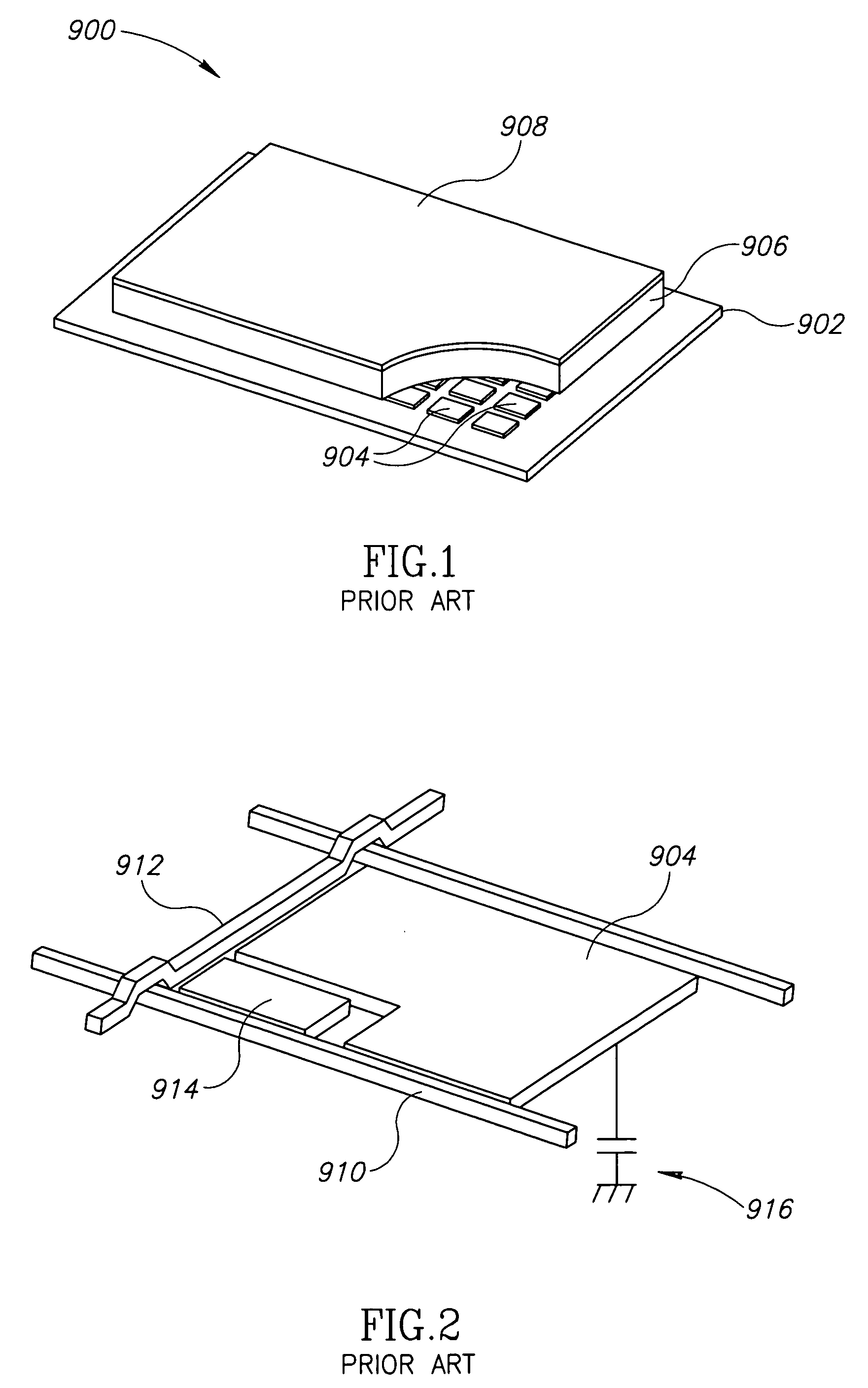
[0023] The use of readout circuitry based on CMOS technology performs better and is less expensive than prior art TFT technology. CMOS circuitry takes advantage of the highly developed manufacturing infrastructure in the semiconductor industry by using the same fabrication processes used to make microprocessors and logic arrays.
[0024] The size of CMOS wafers used in the industry is relative small, 150 or 200 mm diameter. Accordingly, in the present invention, the “basic” CMOS readout unit, typically 10×10 cm, is made buttable on four sides. Several “basic” devices may be combined to form larger mosaics. Sixteen units positioned side-by-side can be used to produce a detector with an area of 40×40 cm. The information lost from missing pixels in the neighborhood of the butting lines can be easily reconstructed by using widely available interpolation methods.
[0025] The use of CMOS technology enables the addition of special features on a pixel-by-pixel basis, vastly improving the performance of the array. The noise levels that are achievable are significantly lower than that of TFT-based readout circuitry, and the CMOS circuits have larger dynamic ranges. In CMOS-based readout circuitries, typical noise levels below 500 electrons are achievable compared to at least 1500-2000 electrons in TFT-based readout systems. CMOS technology also makes it possible to integrate imaging, timing and readout functions all on the same device. The highly integrated architecture allows for the design of a “system on a chip”, which is less costly than an imager requiring large amounts of support electronics.
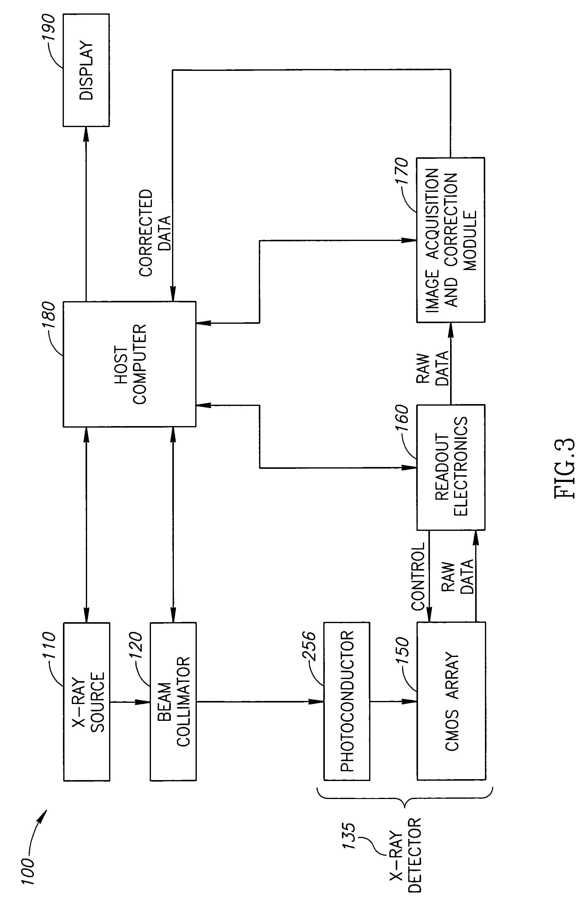
[0030] In a further embodiment of the detector, the plurality of pixels in the array of tiles is internally configured into independent blocks, wherein the pixels in each of the blocks share common readout and control electronics thereby allowing high readout rates. In this embodiment, the independent blocks allow for processing data at a rate of up to about 120 fps.

Problems solved by technology

Despite being widely used, image-intensifier-based fluoroscopic systems have major limitations.
This makes it necessary to significantly increase the size of the device, limiting accessibility to the patient.
A further problem associated with image intensifiers is the degradation of image quality resulting from vignetting, pincushion distortions, etc inherent to this type of device.
Coating materials used in currently available direct-conversion detectors / sensors produce a limited signal because the amount of charge generated as a consequence of the absorption of X-ray is limited.
Formation of such a thick photoconductive layer takes a long time, and further, management of the fabrication process is complex.
This results in extremely low productivity and high manufacturing costs.
Flat panel detectors of the indirect type present significant limitations as well.
A major problem associated with indirect-conversion detectors is that the fluorescent light generated by the phosphor spreads in an isotropic manner and arrives at adjacent pixels.
This leads to crosstalk effects and to the deterioration of the spatial resolution of the detected image.
Furthermore, coating materials have a relatively low X-ray sensitivity.
This severely limits the signal-to-noise ratio achievable with indirect-conversion systems.
A further limitation shared by detectors of both the indirect- and direct-conversion types is the use of TFT-based readout circuitries.
TFT readout systems lack pixel amplification and, therefore, small signals have to be transported across the panel to reach off-device amplifiers.
TFT-based readout circuitries also have the disadvantage that a whole line of pixels, rather than individual pixels, are addressed simultaneously.
This severely limits readout speed and increases electronic noise.
These inefficiencies mean that the noise associated with the electronic signal—readout noise—is greater than the signal produced by the fluoroscopic exposure.
The result is degraded image quality which reduces the clinical usefulness of the image.

Method used


Image

  • Two-dimensional CMOS-based flat panel imaging sensor
  • Two-dimensional CMOS-based flat panel imaging sensor
  • Two-dimensional CMOS-based flat panel imaging sensor

Examples


Embodiment Construction

[0058] In what is described herein, “detector”, “sensor” and “imager” and words derived therefrom such as “sensing”, “detecting” and “imaging” will be used interchangeably. Unless the contrary is indicated, there will be no attempt to distinguish between these terms.

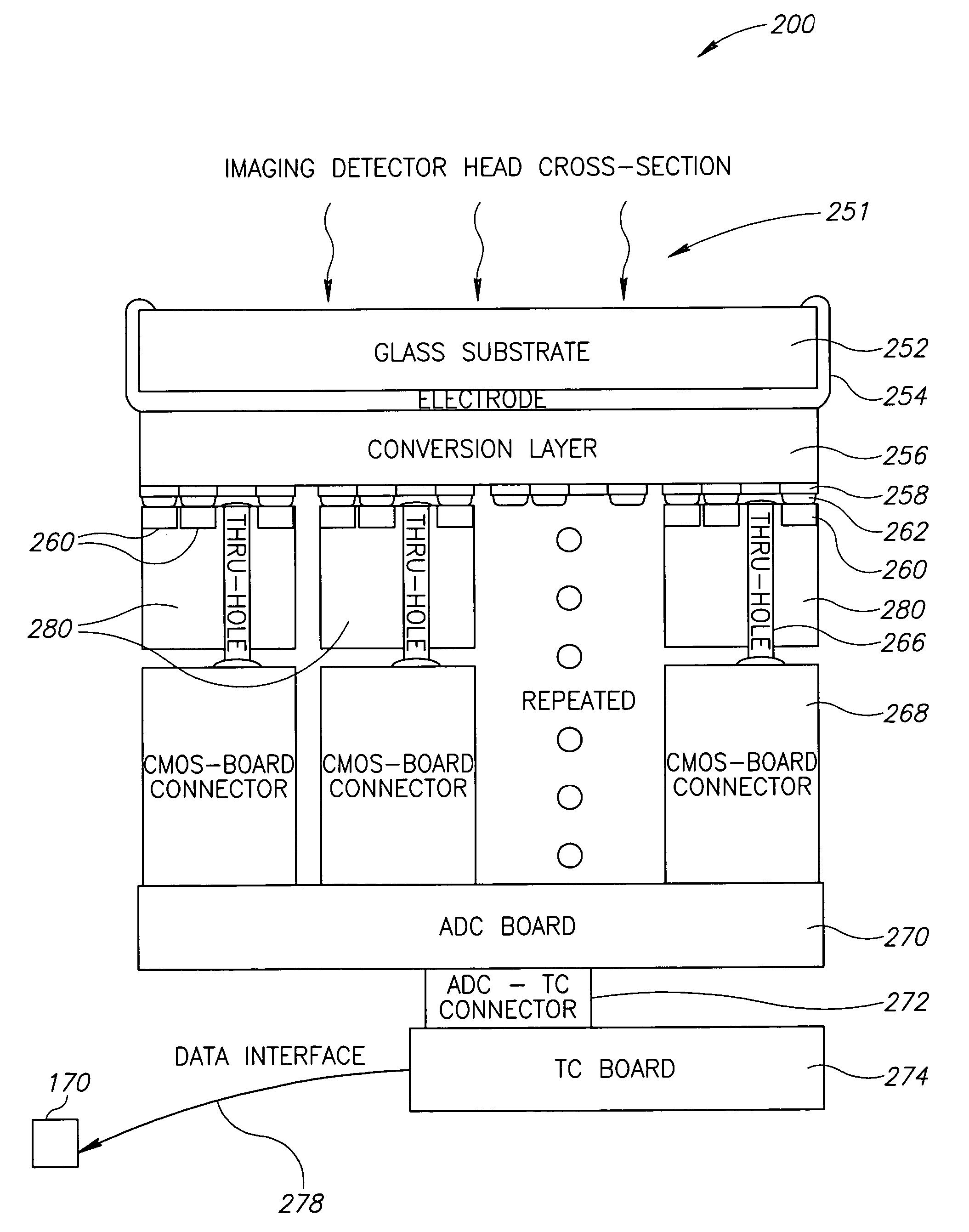
[0059] A flat-panel sensor of a direct-conversion type is herein proposed, wherein the sensor overcomes the problems inherent in both prior art indirect-conversion and direct-conversion sensors discussed above. The sensors discussed herein include high-speed CMOS-based readout circuitry. In the planar sensors of the present invention, incident X-rays are directly converted into electric charges which are then amplified and stored in each pixel of the sensor. The sensor incorporates a large-area CMOS tile array, each tile having four side abuttability and inter-tile distances of about a pixel. Four side abuttability as used herein is defined as a construction wherein tiles may be placed along the four borders of a given ...


PUM


Abstract

The present invention provides a large-area flat plate detector. The detector includes a conversion layer which converts incident electromagnetic radiation into electric charges. The detector has a first electrode in communication with the conversion layer and a second electrode formed as a plurality of pixels arranged in a matrix. The detector includes an array of CMOS tiles, each of the tiles comprised of a plurality of pixels and having four side abuttability. The tile array is configured so that each of the tiles is separated by a spacing equal to about one pixel length from every adjacent tile and internally configured to allow for a high readout rate. Each of the tile pixels is arranged in electrical communication with and mapped in one-to-one fashion with the pixels of the second electrode. The readout electronics is capable of reading out CMOS provided data at a rate of at least 30 fps.

Description

FIELD OF THE INVENTION [0001] The present invention relates to a two-dimensional flat panel sensor for detecting and imaging electromagnetic radiation, typically, but without being limiting, X-ray radiation. BACKGROUND OF THE INVENTION [0002] X-ray imaging has long been an accepted medical diagnostic tool. The oldest and still the most common form of X-ray imaging is conventional (still) radiography. In this modality, a burst of X-ray radiation produced by a high voltage vacuum tube irradiates a body region of clinical interest. The X-rays pass through that portion of the patient's body and a film is used to capture a still image. The exposed film is then chemically processed to create a visible image for diagnosis. Conventional radiography is commonly used to capture, as examples, thoracic, cervical, spinal, cranial, and abdominal images. [0003] By the early 1960s X-ray technology had progressed to the point where dynamic imaging—moving rather than still pictures—became possible. T...

Claims


Application Information

Patent Timeline
IPC IPC(8): G01J1/42H01J40/14
CPCG01J1/4228G01T1/2928H01L27/14676H04N5/32G01T1/247H04N25/30H04N25/00
Inventor KUSZPET, MARIODUKEMAN, SHAULBRUNING, HORST F.PHIPPS, NEIL T.
Owner REAL TIME RADIOGRAPHY
Learn More