Organic electroluminescent element

a technology of electroluminescent elements and organic materials, which is applied in the direction of discharge tubes/lamp details, luminescent screens of discharge tubes, natural mineral layered products, etc., can solve the problems of phosphorescent materials inevitably deteriorating, reducing driving durability and light emission efficiency, and achieve excellent driving durability , high luminescent efficiency, the effect of improving driving durability

Inactive Publication Date: 2006-08-31
UDC IRELAND
View PDF7 Cites 51 Cited by
  • Summary
  • Abstract
  • Description
  • Claims
  • Application Information

AI Technical Summary

Benefits of technology

[0010] The inventor, after variously studying, found that when at least two host materials and at least two phosphorescent materials are included in a luminescent layer and when energy levels such as the electron affinities and the ionization potentials thereof are set in particular ranges, the high luminescent ef...

Problems solved by technology

However, in the luminescent element described in JP-A Nos. 2002-313583 and 2002-324673, since carriers are trapped by a phosphorescent material, the phosphorescent mate...

Method used


Image

  • Organic electroluminescent element
  • Organic electroluminescent element
  • Organic electroluminescent element

Examples


example 1

[0162] To one where on a glass substrate an indium / tin oxide (ITO) transparent conductive film was deposited by 150 nm (manufactured by Geomatic Co., Ltd.), by use of photolithography and hydrochloric acid etching, the patterning was applied and thereby a anode was formed. The patterned ITO substrate, after washing in an order of ultrasonic washing with acetone, water washing with pure water and ultrasonic washing with isopropyl alcohol, was dried under nitrogen blow, finally followed by UV ozone cleaning, and was disposed in a vacuum deposition unit. Thereafter, the vacuum deposition unit was evacuated to a degree of vacuum of 2.7×10⁻⁴ Pa or less.

[0163] Subsequently, in the deposition unit, copper phthalocyanine (CuPc) shown below was heated and deposited at a deposition speed of 0.1 nm / sec, and thereby a hole injecting layer having a film thickness of 10 nm was formed.

[0164] In the next place, on the hole injecting layer formed according to the above, 4,4′-bis[N-(1-naphtyl)-N-p...

example 2

[0177] An organic EL element was prepared and measured in the same manner as in example 1, except that a mixture (75:25 by weight ratio) of a hole transporting host 3 below and an electron transporting host 2 below was used as the host materials contained in a luminescent layer.

[0178] The maximum wavelength of a light emission spectrum of the element obtained according to example 2 was 584 nm and identified to be derived from the dopant B.

Electron Transporting Host 2

example 3

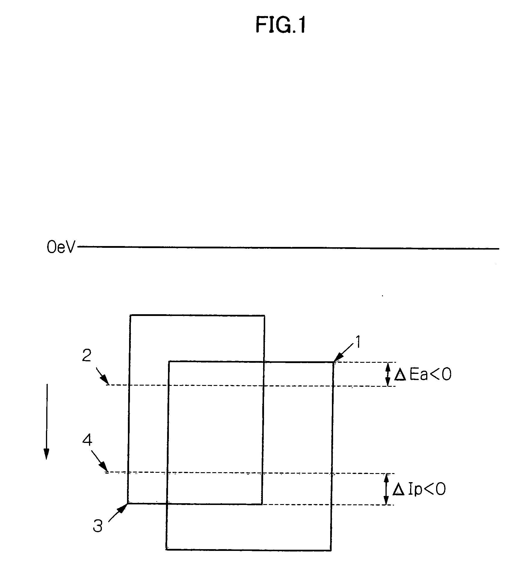
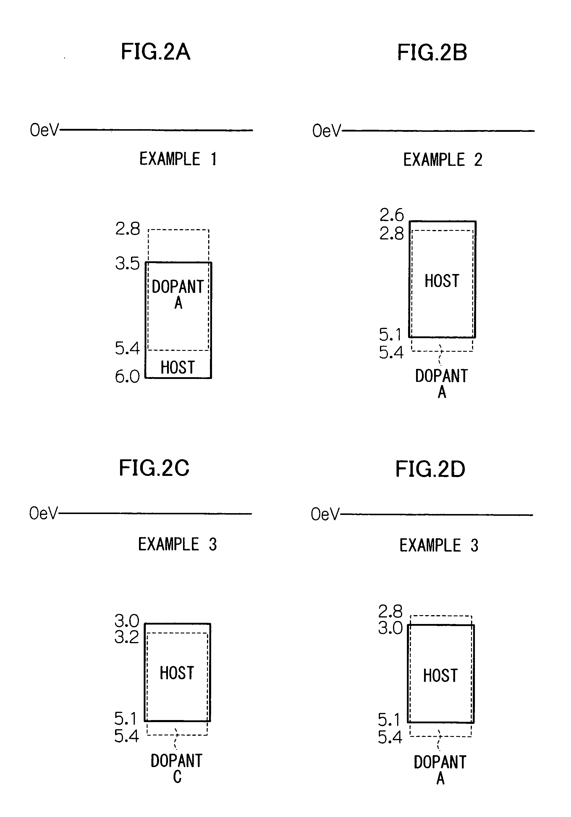
[0184] An organic electroluminescent element was prepared in the same manner as in example 1, except that, as the host materials contained in a luminescent layer, a mixture (75:25 by weight ratio) of a hole transporting host 3 and an electron transporting host 3 shown below, and as phosphorescent organic metal complexes as the dopant materials, the tris(2-phenylpyridine)iridium (dopant A) and an iridium complex (dopant C) below were heated, and a luminescent layer was formed by use of a ternary simultaneous vapor deposition method. Relationships between the ionization potentials and the electron affinities of the phosphorescent materials and the host materials are shown in Table 2. Furthermore, energy states of example 3 are shown in FIGS. 2C and 2D.

TABLE 2Phosphorescent materialCPhosphorescent materialAHost material (mixingHole transporting hostratio)3:Electron transporting host 3 (75:25)Ip(D1) (eV)5.4Ip(D2) (eV)5.4Ip(H)min (eV)5.1Ip(H)min (eV)5.1ΔIp1: Ip(D1) − Ip(H)min0.3ΔIp2: I...


PUM

PropertyMeasurementUnit
Energyaaaaaaaaaa
Energyaaaaaaaaaa
Energyaaaaaaaaaa

Abstract

An organic electroluminescent element including one or more organic compound layers including at least one luminescent layer between an anode and a cathode, wherein the luminescent layer includes at least two host compounds and at least two phosphorescent materials, and the phosphorescent materials include a phosphorescent material (D1) that satisfies at least one of the following conditions: (a) when the ionization potential of the phosphorescent material (D1) is defined as Ip(D1) and the minimum value out of the ionization potentials of the at least two host compounds as Ip(H)min, ΔIp1 as defined by ΔIp1=Ip(D1)−Ip(H)min satisfies ΔIp1<0 eV, and (b) when the electron affinity of the phosphorescent material (D1) is defined as Ea(D1) and the maximum value out of the electron affinities of the at least two host compounds as Ea(H)max, ΔEa1 as defined by ΔEa1=Ea(H)max−Ea(D1) satisfies ΔEa1<0 eV.

Description

CROSS-REFERENCE TO RELATED APPLICATION [0001] This application claims priority under 35 USC 119 from Japanese Patent Application No. 2005-055049, the disclosure of which is incorporated by reference herein. BACKGROUND OF THE INVENTION [0002] 1. Field of the Invention [0003] The present invention relates to an organic electroluminescent element (hereinafter sometimes referred to as an “organic EL element”, a “luminescent element” or an “EL element”) capable of emitting light by converting electric energy into light. [0004] 2. Description of the Related Art [0005] Today, research and development for various display devices is being aggressively pursued and, in particular, organic electroluminescent (EL) elements are attracting attention as promising display devices because high brightness light can be emitted with a low voltage. [0006] A technique of using two or more compounds for the host material of the luminescent layer and using each compound as an electron transporting host or a...

Claims


Application Information

Patent Timeline
IPC IPC(8): H01L51/54H05B33/14
CPCH01L51/0059H01L51/0067H01L51/0071H01L51/0072H01L51/0085H01L51/0087H01L51/5016H10K85/631H10K85/346H10K85/654H10K85/657H10K85/342H10K85/6572H10K50/11H10K2101/10
Inventor NARIYUKI, FUMITO
Owner UDC IRELAND
Why Eureka
Try Eureka