Method for forming interlayer dielectric film in semiconductor device

a technology of semiconductor devices and dielectric films, which is applied in the direction of coatings, metallic material coating processes, chemical vapor deposition coatings, etc., can solve the problems of reducing the refresh property, deteriorating the characteristics of the semiconductor diode, and further damage to the wafer, so as to reduce current leakage and enhance the electric properties of the device.

Inactive Publication Date: 2006-09-14
SK HYNIX INC
View PDF5 Cites 10 Cited by
  • Summary
  • Abstract
  • Description
  • Claims
  • Application Information

AI Technical Summary

Benefits of technology

[0011] The present invention has been made to solve the above problems, and it is an object of the present invention to provide a method for forming an interlayer dielectric film in a semiconductor device, which suppresses an increase in current leakage of a semiconductor device due to plasma, thereby enhancing electric properties of the device.

Problems solved by technology

However, when heating the wafer at a temperature of 850° C., the characteristics of the semiconductor diode are deteriorated.
However, the method as described above has problems in that the wafer is damaged by the plasma during the process of forming the HPD oxide film, and in that the wafer is further damaged by the other plasma processes subsequently performed thereafter or that the refresh property is lowered in the case of a semiconductor memory device, such as a dynamic random access memory (DRAM), due to current leakage caused by a hump property.
Moreover, during the process of forming the HDP oxide film 140, carriers, for example electrons, can be accumulated in a gate oxide film through the metallic wires due to the plasma, and in this case, the current leakage is created at a lower gate, thereby deteriorating the refresh characteristic of the device.

Method used


Image

  • Method for forming interlayer dielectric film in semiconductor device
  • Method for forming interlayer dielectric film in semiconductor device
  • Method for forming interlayer dielectric film in semiconductor device

Examples


Embodiment Construction

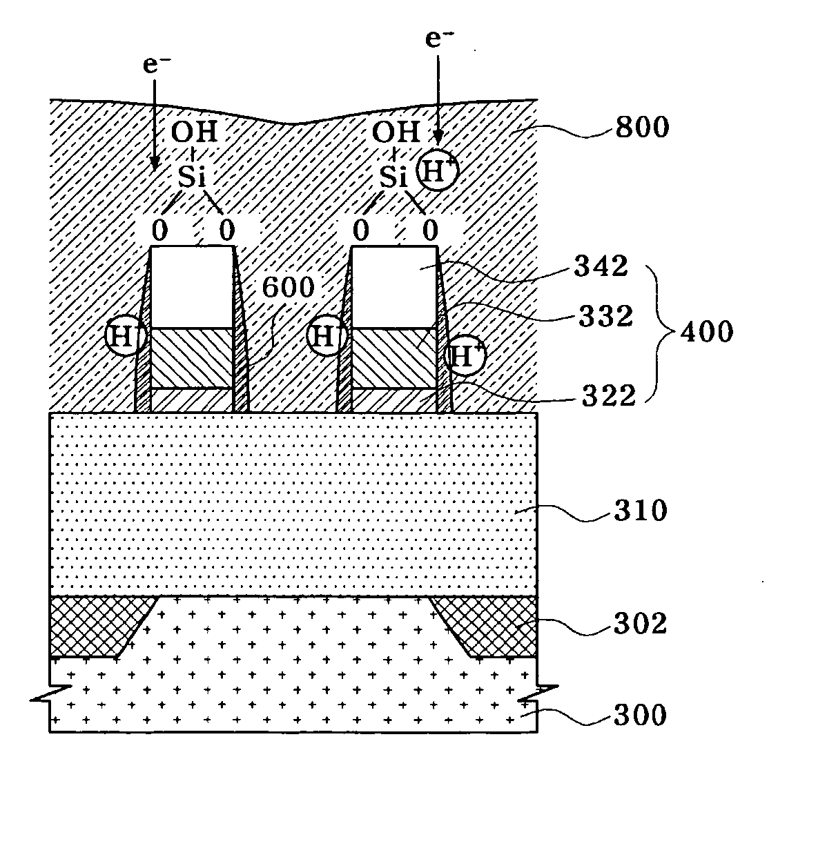
[0028] Reference will now be made in detail to the embodiments of the present invention with reference to the accompanying drawings. It should be appreciated that the present invention can be realized in various shapes, and is not limited to the embodiment described herein. In the drawings, components are enlarged for clear description, and like components are denoted by like reference numerals throughout.

[0029] FIGS. 4 to 8 are cross-sectional views illustrating a method for forming an interlayer dielectric film in a semiconductor device according to the present invention.

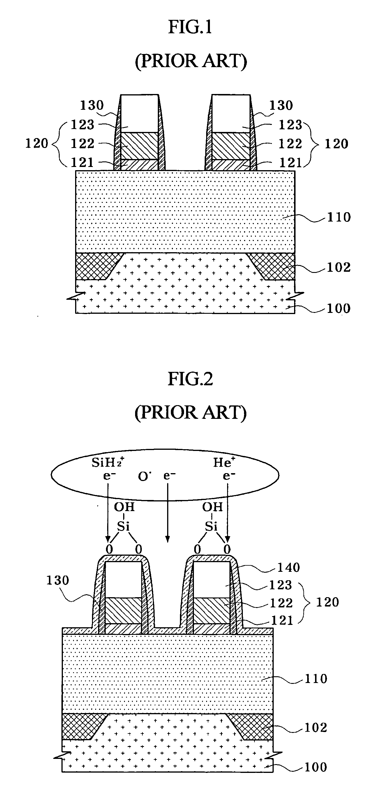
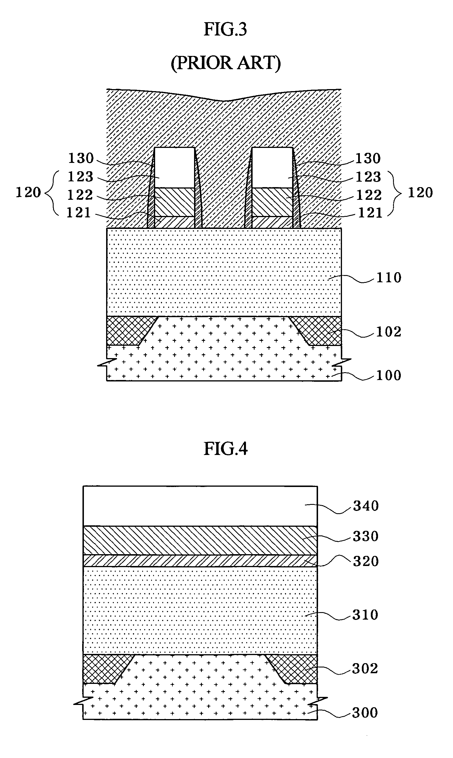
[0030] First, referring to FIG. 4, a first interlayer dielectric film 310 is located on a semiconductor substrate 300 having an active region restricted by a trench isolation layer 302.

[0031] Then, a titanium / titanium nitride (Ti / TiN) layer is deposited as a barrier layer 320 on the first interlayer dielectric film 310, and a tungsten (W) layer is deposited as a metallic layer 330 on the barrier layer 320. Then...


PUM

PropertyMeasurementUnit
temperatureaaaaaaaaaa

Abstract

Disclosed herein is a method for forming an interlayer dielectric film in a semiconductor device. The method comprises the steps of preparing a semiconductor substrate having a dielectric film and conductive film patterns sequentially deposited thereon, and depositing a high plasma oxide film as the interlayer dielectric film on the conductive film patterns and the dielectric films by supplying H2 as an adding gas together with a source gas. A dangling bond in an interface of the semiconductor substrate is reduced by adding hydrogen into the dielectric film, thereby enhancing the uniformity of the deposition. Moreover, hydrogen in the dielectric film decreases current leakage occurring in the gate by preventing electrons in the plasma from flowing into a gate through the bit-line, thereby enhancing the refresh characteristics of the semiconductor device.

Description

BACKGROUND OF THE INVENTION [0001] 1. Field of the Invention [0002] The present invention generally relates to a method for manufacturing a semiconductor device, and, more particularly, to a method for forming an interlayer dielectric film of a semiconductor device. [0003] 2. Description of the Related Art [0004] Recently, as semiconductor diodes have become highly integrated, resulting in a gradual decrease in the design rule thereof, the gap between conductive patterns has also been narrowed. As a result, an importance of a gap-filling method for completely filling the gap between conductive patterns with an interlayer dielectric film covering the conductive patterns is emphasized. Generally, the interlayer dielectric film is formed by a chemical vapor deposition (CVD) process. When forming the interlayer dielectric film by use of a typical CVD process, an additional process of heat treating a wafer at a high temperature is performed after depositing the interlayer dielectric film...

Claims


Application Information

Patent Timeline
Patent Type & Authority Applications(United States)
IPC IPC(8): H01L21/4763
CPCC23C16/402H01L21/02164H01L21/02274H01L21/0234H01L21/31608H01L21/76837H01L21/205
Inventor CHUNG, JIE WON
Owner SK HYNIX INC
Why Eureka
Try Eureka