Forming solder balls on substrates

a technology of substrates and solder balls, which is applied in the direction of soldering apparatus, non-printed masks, semiconductor/solid-state device details, etc., can solve the problems of limiting the usefulness of the technique, high cost of cleaning processing equipment and replacing metal masks, and not well suited to fine-pitch ball bumping, etc., to achieve easy scaling to lower the densities of large solder balls, high densities of small solder balls, and low capital expenditure equipmen

Inactive Publication Date: 2006-09-21
SEMIPAC INC
View PDF75 Cites 23 Cited by
  • Summary
  • Abstract
  • Description
  • Claims
  • Application Information

AI Technical Summary

Benefits of technology

[0047] The process of the present invention is capable of achieving high densities of small solder balls, and is readily scaleable to lower densities of large solder balls. The process proceeds relatively quickly, with low capital expenditure equipment, and without hazardous chemicals.
[0048] The present invention provides a fast, low-cost, robust, non-capital-intensive method and apparatus for forming arrays of solder bumps at moderate to high densities on electronic components, including 150 μm area arrays, 200 μm area arrays, and 250 μm area arrays, forming solder balls at 0.5 mm pitch and at 0.8 mm pitch.

Problems solved by technology

A number of techniques are known for ball bumping electronic components, some of which are not well suited to fine pitch ball bumping.
This requires a high investment in capital equipment and has high cost associated with cleaning the processing equipment and with replacing the metal mask on a frequent basis.
Thermal mismatch between the evaporation mask and the substrate being ball bumped tends to limit the usefulness of the technique to moderate densities and moderate solder bump sizes.
This technique is time consuming, requires high capital expenditure, and involves hazardous chemicals.
This technique is relatively inexpensive, and comprises only a few quick steps, but is generally not well suited to small bump sizes and high bump densities.
The advent and popularity of the BGA package has brought with it several new package manufacturing and assembly problems.
One of the more significant problems is finding an efficient, cost-effective technique for applying the solder balls to the package surface.
Difficulties with any technique involving measuring or dispensing precise quantities of solder paste on pads to form ball bumps include dealing with the rheological characteristics (elasticity, viscosity, plasticity) of the solder paste, accurately controlling the volume of solder paste after dispensing and reflow, and the shape of the final ball bump.
As mentioned above, in general it is difficult to form contacts with height-to-width ratios (aspect ratios) of greater than 1:1.
Some techniques involving “building up” of solder contact height in a series of process steps have managed to produce tall (high aspect ratio) contacts, but such techniques are typically expensive and cumbersome in high-volume production.
If one or more of the solder balls are significantly shorter than others (usually due to an insufficient amount of solder paste deposited on one or more conductive pads prior to contact formation) it becomes highly likely that these smaller (shorter) contacts will completely miss their mating contact pads (on the circuit board) and will fail to form an electrical connection between the packaged semiconductor device and the underlying substrate (e.g., printed circuit board).
Defective assemblies of packages to interconnection substrates can be difficult or impossible to repair after assembly if connections are not properly formed.
Even prior to assembly, the correction of improperly formed solder balls on the exterior of a package can be very difficult and involves, initially, careful quality control inspection of the ball bumps prior to assembly of the packaged device to a substrate.
As the volume of packages produced by the aforementioned methods increases, the complexity of the manufacturing processes becomes an obstacle to high manufacturing rates.
Generally speaking, complicated setup and tooling changes tend to increase downtime, thereby increasing production cost.

Method used


Image

  • Forming solder balls on substrates
  • Forming solder balls on substrates
  • Forming solder balls on substrates

Examples


Embodiment Construction

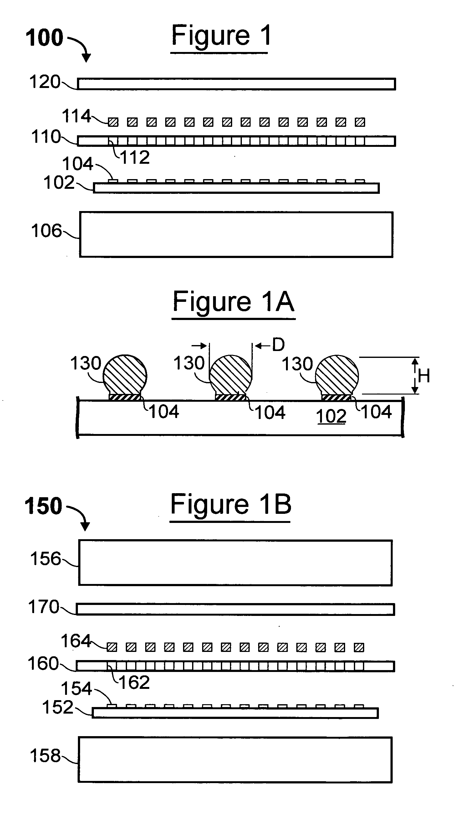
[0108]FIG. 1 illustrates a technique 100 for forming solder balls on a surface of a substrate 102, such as is set forth in “parent” U.S. patent application Ser. No. 08 / 863,800 (U.S. Pat. No. 5,988,487, Nov. 23, 1999), incorporated in its entirety by reference herein.

[0109] The substrate 102 has number of pads 104 on its top (as viewed) surface. The pads 104 are typically arranged in an array, having a pitch (center-to-center spacing from one another). The substrate 102 is disposed atop a heater stage 106.

[0110] A mask (stencil) 110 is provided. The mask 110 is a thin planar sheet of relatively stiff material, such as molybdenum, having a plurality of openings (cells) 112, each corresponding to a pad 104 whereupon it is desired to form a solder ball on the substrate 102.

[0111] The mask 110 is placed on the top (as viewed) surface of the substrate 102 with the cells 112 aligned over the pads 104. The cells 112 in the mask 110 are filled with solder material 114. This is done in any...


PUM

PropertyMeasurementUnit
diameteraaaaaaaaaa
diameteraaaaaaaaaa
diameteraaaaaaaaaa

Abstract

A mask (stencil) having cells (openings) is disposed on a surface of a heater stage, and is then filled (printed) with solder paste. Then a substrate is assembled to the opposite side of the mask. Then the solder paste is reflowed. This may be done partially inverted. Then the mask is separated from the substrate, either before or after cooling. Solder balls are thus formed on the substrate, which may be a semiconductor wafer. A biased chuck urges the substrate into intimate contact with the mask. A method for printing the mask with solder paste is described. Methods of forming high aspect ratio solder bumps (including balls and reflowable interconnect structures) are described.

Description

CROSS-REFERENCES TO RELATED APPLICATIONS [0001] This is a continuation of U.S. Ser. No. 10 / 643,766 filed Aug. 18, 2003 (issuing as U.S. Pat. No. 7,007,833). [0002] U.S. Ser. No. 10 / 643,766 is a continuation-in-part of: [0003] Ser. No. 09 / 962,007 filed Sep. 24, 2001 (U.S. Pat. No. 6,609,652, Aug. 26, 2003) [0004] which is a continuation-in-part of: [0005] U.S. Ser. No. 09 / 273,517 filed Mar. 22, 1999 (U.S. Pat. No. 6,293,456, Sep. 25, 2001), [0006] which is a continuation-in-part of each of: [0007] U.S. Ser. No. 08 / 863,800 filed 27 May 1997 (U.S. Pat. No. 5,988,487, Nov. 23, 1999); [0008] U.S. Ser. No. 60 / 079,006 filed 23 Mar. 1998; [0009] U.S. Ser. No. 60 / 079,221 filed 24 Mar. 1998; and [0010] U.S. Ser. No. 60 / 092,055 filed 8 Jul. 1998, all of which are incorporated in their entirety by reference herein. [0011] U.S. Ser. No. 10 / 643,766 is also a continuation-in-part of: [0012] U.S. Ser. No. 10 / 630,310 filed Jul. 30, 2003 as a continuation-in-part of the aforementioned Ser. No. 09 / 96...

Claims


Application Information

Patent Timeline
Patent Type & Authority Applications(United States)
IPC IPC(8): B23K35/12B23K1/00B23K3/06B23K3/08B23K35/02B23K35/22H01L21/48H01L21/60H05K3/34
CPCB23K1/0016B23K3/0623B23K3/0638B23K3/087B23K35/0222B23K35/0244B23K35/22B23K35/224B23K2201/40B23K2201/42H01L21/4853H01L24/11H01L2224/0401H01L2224/0603H01L2224/11003H01L2224/1147H01L2224/13022H01L2224/131H01L2224/1403H01L2224/16H01L2924/01013H01L2924/01015H01L2924/01027H01L2924/01029H01L2924/01042H01L2924/01074H01L2924/01075H01L2924/01082H01L2924/01322H01L2924/14H01L2924/19041H05K3/3484H05K2201/10477H05K2203/0113H05K2203/0278H05K2203/0338H05K2203/043H05K2203/0557H05K2203/085H05K2203/1581H01L2924/014H01L2224/13011H01L2224/1613H01L2924/00013H01L2924/01005H01L2924/01006H01L2924/01033H01L2224/13099H01L2224/1131H01L2224/11334B23K2101/40B23K2101/42H01L24/05H01L24/13H01L2224/05551H01L2224/05553H01L2224/05554H01L2224/14H01L2224/14051H01L2924/351H05K3/3485H01L2924/00
Inventor MACKAY, JOHNMOLINARO, TOM
Owner SEMIPAC INC
Why Eureka
Try Eureka