Microlens array substrate and production method therefor

a technology of micro-lens array and substrate, which is applied in the field of micro-lens array substrate, can solve the problems of increasing the ratio of this non-lens area, difficult to form the micro-lens array, and difficulty in controlling the pattern size of the micro-lens array, so as to achieve the effect of reducing the amount of material used, simplifying the structure and accurate pattern siz

Inactive Publication Date: 2006-09-28
SONY CORP
View PDF3 Cites 34 Cited by
  • Summary
  • Abstract
  • Description
  • Claims
  • Application Information

AI Technical Summary

Benefits of technology

[0020] According to the micro-lens array substrate of the present invention, since the micro-lens array having the plurality of consecutive concave lens shapes is directly formed in the surface of the quartz substrate or glass substrate by the transfer method based on the dry-etching, a micro-lens array substrate that has a precise micro-lens array whose pattern size is accurate can be provided. Since this micro-lens array is formed by filling the lens-shaped concave portion formed in the surface of the quartz substrate or glass substrate with the resin layer of the different refractive index, a material to be used can be reduced and a structure can be simplified.
[0021] According to the micro-lens array substrate of the present invention, since the taper portion is provided toward the surface of the substrate in the peripheral portion of the micro-lens array on the micro-lens array substrate, an excellent micro-lens array substrate can be formed without generating an air bubble and distortion by reducing the shrinkage of the micro-lens array and peripheral portion when the cover glass is bonded and the resin is hardened after the resin is filled. Since the air bubble is not generated, it is possible to use a micro-lens in the outermost circumference of the micro-lens array.
[0022] According to the method for manufacturing the micro-lens array substrate of the present invention, the micro-lens array is formed by transferring the lens-shaped concave p

Problems solved by technology

However, it is difficult to control a pattern size of the micro-lens array due to a thermal shrinkage of the resin layer 45 at the time of hardening.
Particularly, when the micro-lens itself is made minute in order to obtain higher resolution, a ratio of this non-lens area increases and it becomes difficult to form the micro-lens array.
Also, there have been limits in thermostability and light stability since two kinds of resins are used.
In the method for manufacturing the micro-lens array substra

Method used


Image

  • Microlens array substrate and production method therefor
  • Microlens array substrate and production method therefor
  • Microlens array substrate and production method therefor

Examples


first embodiment

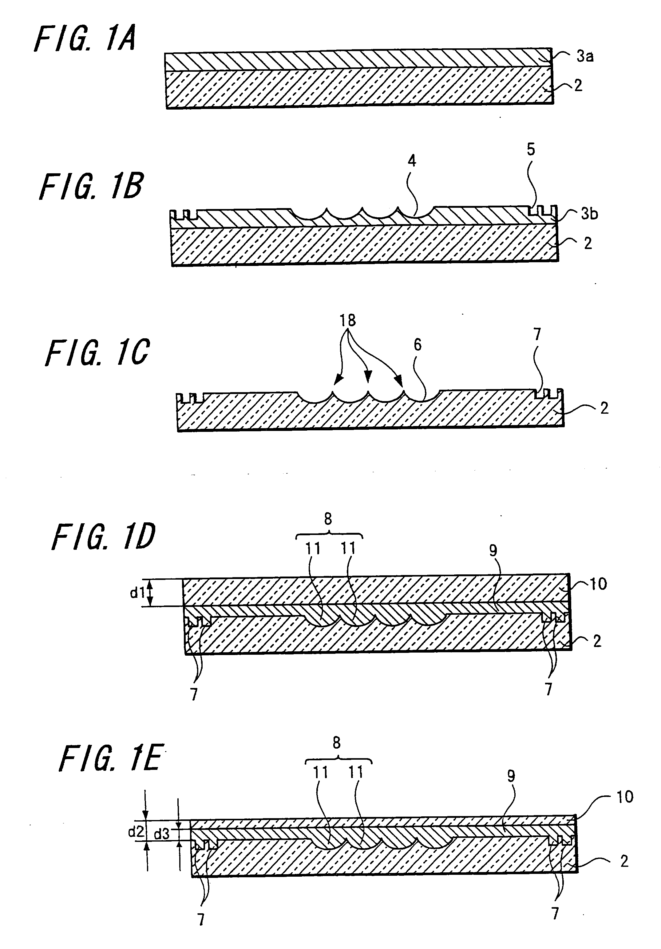
[0083] A first embodiment of a micro-lens array substrate and a method for manufacturing thereof according to the present invention is shown in FIGS. 1 and 2. In this embodiment, an explanation is made to a micro-lens array substrate for a liquid crystal panel constituting a liquid crystal projector.

[0084] First, as shown in FIG. 1A, a quartz substrate or glass substrate of a parallel plate that is a transparent substrate, which is a quartz substrate 2 in this embodiment, is prepared. A photo-resist layer 3a having a required thickness is formed on a surface of this parallel plate of the quartz substrate. In this embodiment, the photo-resist layer 3a is formed by a spin coat method.

[0085] Next, as shown in FIG. 1B, with performing a photolithography treatment (pattern exposure and development process) on the photo-resist layer 3a, a resist layer 3b having on the surface a concave-shaped curved surface (hereinafter, referred to as a lens-shaped concave portion) 4 of a plurality of ...

second embodiment

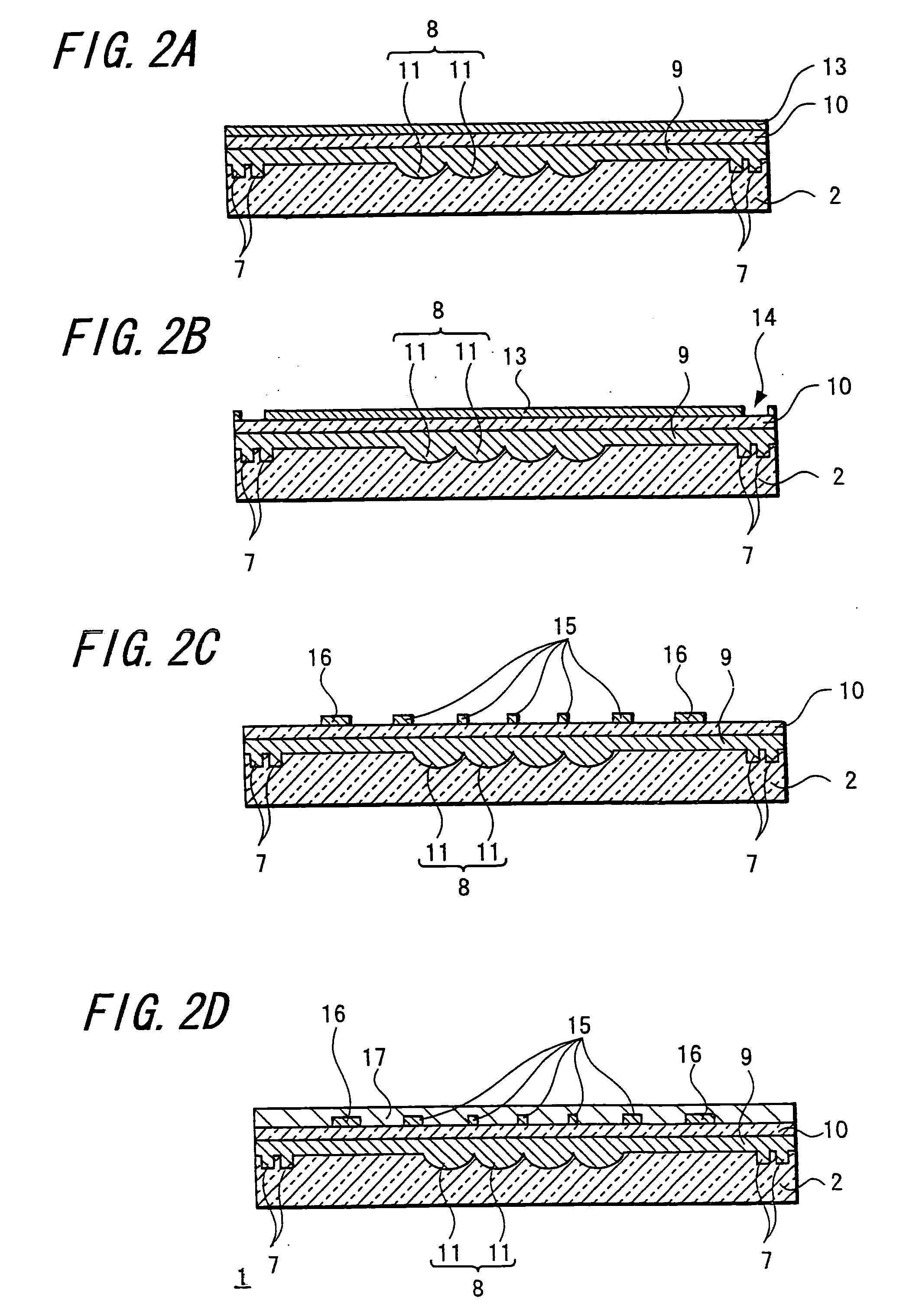
[0107] Next, a second embodiment of a micro-lens array substrate and a method for manufacturing thereof according to the present invention is shown in FIGS. 3 and 4. This embodiment is also a case in which the present invention is applied to a micro-lens array substrate used for a liquid crystal panel constituting a liquid crystal projector.

[0108] In this embodiment, since processes from FIGS. 3A to 3C are similar to the above-described processes from FIGS. 1A to 1C, a redundant explanation thereof is omitted.

[0109] In this embodiment, as shown in FIG. 3D, the alignment mark 16 for bonding a TFT substrate on the surface of the quartz substrate 2 is formed after the process of FIG. 3C. For example, an aluminum film for example is formed on the whole surface of the quartz substrate 2 in the same manner as described above, and an opening is formed by selectively etching and removing the aluminum film at the portion corresponding to the alignment mark 7 for stepper. Subsequently, a po...

third embodiment

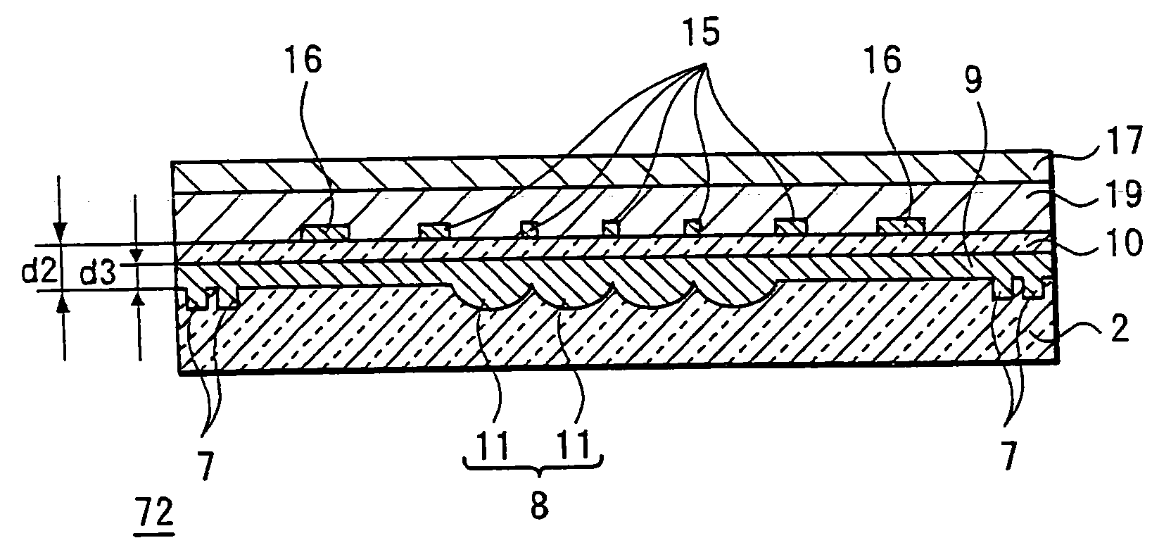
[0114] A third embodiment of a micro-lens array substrate 72 according to the present invention is shown in FIG. 5.

[0115] This embodiment is also a case in which the present invention is applied to a micro-lens array substrate used for a liquid crystal panel constituting a liquid crystal projector.

[0116] In this embodiment, since the processes are the same as those shown in FIGS. 1A through 2C, a redundant explanation thereof is omitted.

[0117] In this embodiment, as shown in FIG. 5, a transparent protective layer that is a silicon oxide film (SiO2 film) 19, for example, is formed after the process of FIG. 2C on the cover glass plate 10 in which the black matrix 15 and alignment mark 16 are formed, and a transparent conductive layer that is the opposing electrode 17 made of the ITO (Indium Tin Oxide) film, for example, is formed as a further upper layer to obtain the objective micro-lens array substrate 72 of a parallel plate.

[0118] In the micro-lens array substrate 72 and method...


PUM


Abstract

A micro-lens substrate having a precise micro-lens array suitable for higher resolution, the micro-lens array substrate of high quality without having a distortion, and a method for manufacturing thereof are provided. In the micro-lens array substrate of the present invention, a micro-lens array formed of a plurality of consecutive concave lens-shaped micro-lenses is directly formed in a surface of a quartz substrate or glass substrate, and the micro-lens array is formed by a transfer method based on dry-etching. In the micro-lens array substrate of the present invention, a taper portion is formed toward the surface of the substrate in a peripheral portion of the micro-lens array in the quartz substrate or glass substrate. In a method for manufacturing the micro-lens array substrate of the present invention, a resist layer having a plurality of consecutive lens-shaped concave portions is formed in a surface of a quartz or glass substrate, the lens-shaped concave portion of the resist layer is transferred to the substrate by dry-etching, and a micro-lens array is formed by injecting a resin into the lens-shaped concave portion of this substrate. In addition, a taper portion is formed in a peripheral portion similarly to the formation of the lens-shaped concave portion, and a micro-lens array is formed by injecting a resin into the lens-shaped concave portion and taper portion.

Description

TECHNICAL FIELD [0001] The present invention relates to a micro-lens array substrate used for a liquid crystal projector and a method for manufacturing thereof. BACKGROUND ART [0002] A front AV projector device which has been used for business is gaining ground in a consumer market of a home theater system, for example, with the development of a low-price liquid crystal projector. In the liquid crystal projector, a size thereof has rapidly been reduced and a price thereof has been reduced by improving a degree of integration of components. In addition, a resolution has also been improved with VGA, SVGA, XGA, and SXGA because of the progress of a personal computer, and so a micro-lens array substrate that projects an image of a liquid crystal monitor by efficiently using light from a light source is required also with the improvement in the resolution of the liquid crystal monitor installed in the liquid crystal projector. [0003] In this micro-lens array substrate, a degree of integr...

Claims


Application Information

Patent Timeline
IPC IPC(8): G02B27/10G02B3/00G02B3/02G02F1/1333G02F1/1335
CPCG02B3/0012G02B3/0031G02B3/0075G02F1/133526
Inventor ABE, MORIAKIMINAMI, HIROYUKISATOH, KENICHISHINODA, KAZUHIROMIZUMA, JUNICHI
Owner SONY CORP
Why Eureka
Try Eureka