Differential transmitter circuit

a transmitter circuit and differential technology, applied in the field of transmitter circuits, can solve the problems of longer off-chip communication paths, more discontinuities, and high noise, and achieve the effect of reducing the overall gain of the amplifier stag

Active Publication Date: 2006-09-28
IBM CORP
View PDF4 Cites 10 Cited by
  • Summary
  • Abstract
  • Description
  • Claims
  • Application Information

AI Technical Summary

Benefits of technology

[0009] Differential amplifier stages may be configured as common source FET stages or common emitter bipolar stages. As the current in each half of the differential stage is varied in response to an input signal, a corresponding voltage change is generated across a load resistor in series with each drain or collector that sets the source resistance of the outputs. The differential stages are normally biased with a circuit that approximates an ideal current source having a current value I. If the two FET devices making up the differential stage are matched, then each stage will conduct current I / 2 with equal input voltages as the current source voltage adjusts to force both devices to have the same gate to source voltage (VGS) and thus the same drain current. When the differential input voltage changes, then one-half of the change appears as an increase to one VGS and the other half appears as a decrease in the other VGS. This causes one drain current to increase and the other to decrease by the same amount while the total current remains equal to current I of the current source. A resistance R is added between the source terminals of the two FET devices to modify the gain of the differential stage. Now, when the differential input voltage changes, part of the change appears as changes in the VGS values as discussed and part appears as voltages across the resistance R. Only the variation in VGS changes the corresponding drain currents and thus the output voltages, therefore, the effect of adding resistance R to the source circuit is to reduce the overall gain of the amplifier stage.

Problems solved by technology

Off-chip communication paths are longer, have higher noise, impedance mismatches, and have more discontinuities than on-chip communication paths.
When using inter-chip high-speed signaling, noise and coupling between signal lines (crosstalk) affects signal quality.
If environmental factors cause the delay of the delay line to vary, then accurately sampling the clock may be compromised or may cause errors.
Simply boosting the high frequency content above a non compensated level may also increase the high frequency noise.

Method used


Image

  • Differential transmitter circuit
  • Differential transmitter circuit
  • Differential transmitter circuit

Examples


Embodiment Construction

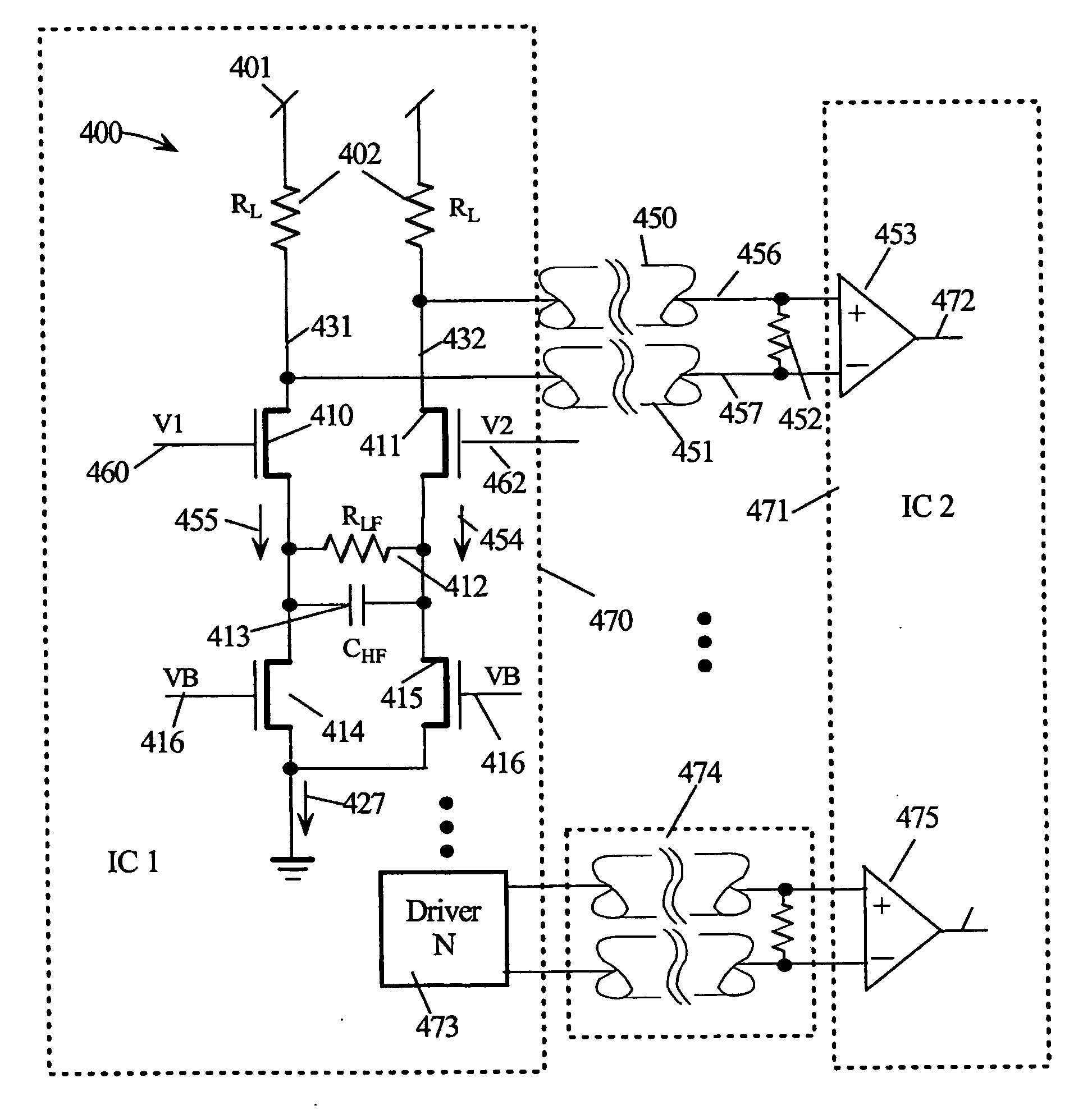
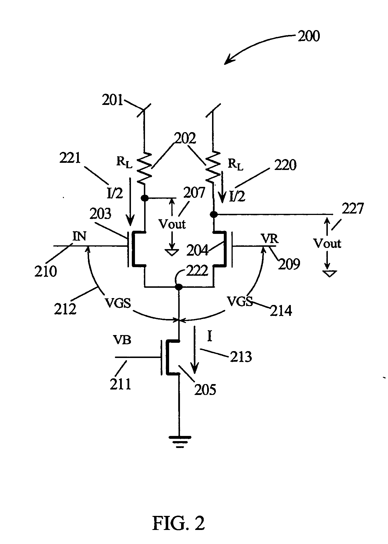
[0021] In the following description, numerous specific details are set forth to provide a thorough understanding of the present invention. However, it will be obvious to those skilled in the art that the present invention may be practiced without such specific details. In other instances, well-known circuits may be shown in block diagram form in order not to obscure the present invention in unnecessary detail. For the most part, details concerning timing considerations and the like have been omitted inasmuch as such details are not necessary to obtain a complete understanding of the present invention and are within the skills of persons of ordinary skill in the relevant art.

[0022] Refer now to the drawings wherein depicted elements are not necessarily shown to scale and wherein like or similar elements are designated by the same reference numeral through the several views.

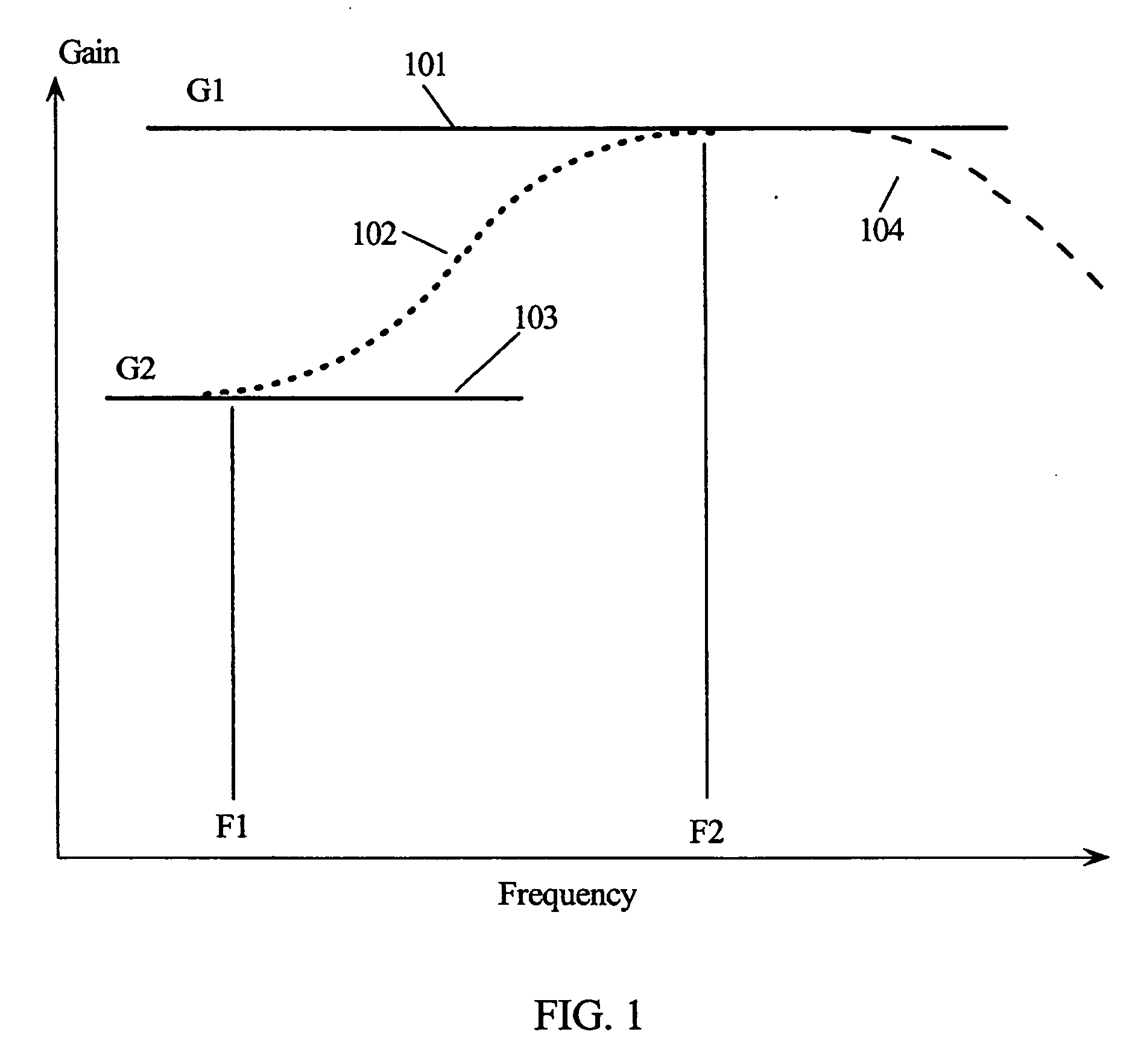
[0023]FIG. 1 illustrates three frequency response curves plotting gain as a function of frequency for a differ...


PUM


Abstract

A driver circuit is configured as a frequency compensated differential amplifier having one input coupled to a first data signal and a second input coupled to a second data signal. Each stage of the differential amplifier is biased with a current source. The driver circuit generates a first output signal coupled to the input of a first transmission line and a second output signal coupled to the input of a second transmission line. The first and second output signals are generated as the difference between the first and second data signals amplified by a compensated gain. A compensation network that attenuates the low frequency components of the input signals relative to the high frequency components is coupled between current sources biasing the differential amplifier. The outputs of the first and second transmission lines are coupled to the inputs of a differential receiver that may or may not be frequency compensated.

Description

CROSS-REFERENCE TO RELATED APPLICATION [0001] This patent application is related to the following commonly owned copending U.S. patent application Ser. No. 11 / 055,806 entitled “Peaking Transmission Line Receipt for Logic Signals,” filed Feb. 11, 2005.TECHNICAL FIELD [0002] The present invention relates in general to board level transmission line drivers and receivers, and in particular, to transmitter circuits for driving transmission lines coupling elements on circuit boards. BACKGROUND INFORMATION [0003] Digital computer systems have a history of continually increasing the speed of the processors used in the system. As computer systems have migrated towards multiprocessor systems, sharing information between processors and memory systems has also generated a requirement for increased speed for the off-chip communication networks. Designers usually have more control over on-chip communication paths than for off-chip communication paths. Off-chip communication paths are longer, have...

Claims


Application Information

Patent Timeline
Patent Type & Authority Applications(United States)
IPC IPC(8): H04L25/00
CPCH03F3/45197H03F2200/543H03F2203/45488H04L25/0274
Inventor HARIDASS, ANANDTRUONG, BAO G.ZIEGELBEIN, JOEL D.
Owner IBM CORP
Why Eureka
Try Eureka