Circuit for detecting and measuring noise in semiconductor integrated circuit

a technology for semiconductor integrated circuits and noise detection, applied in noise figures or signal-to-noise ratio measurement, semiconductor/solid-state device details, instruments, etc., can solve problems such as troublesome tasks, deterioration of detection characteristics, and increase of leading wire length, so as to achieve easy error analysis, no deterioration of detection characteristics, and easy to perform

a technology for semiconductor integrated circuits and noise detection, applied in noise figures or signal-to-noise ratio measurement, semiconductor/solid-state device details, instruments, etc., can solve problems such as troublesome tasks, deterioration of detection characteristics, and increase of leading wire length, so as to achieve easy error analysis, no deterioration of detection characteristics, and easy to perform

US20060221531A1Inactive Publication Date: 2006-10-05THE NEW IND RES ORG

Image

  • Circuit for detecting and measuring noise in semiconductor integrated circuit
  • Circuit for detecting and measuring noise in semiconductor integrated circuit
  • Circuit for detecting and measuring noise in semiconductor integrated circuit

Examples


first embodiment

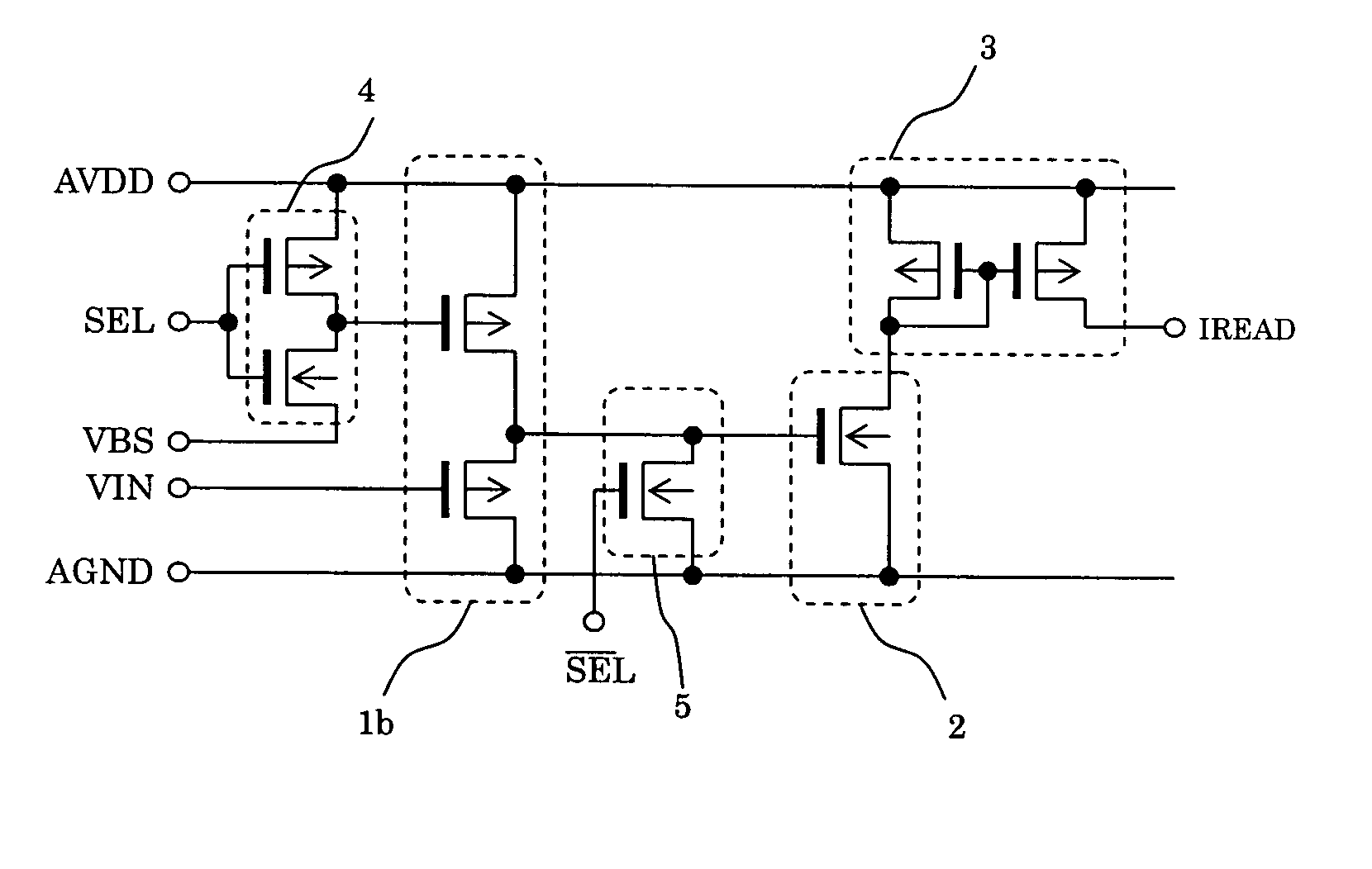
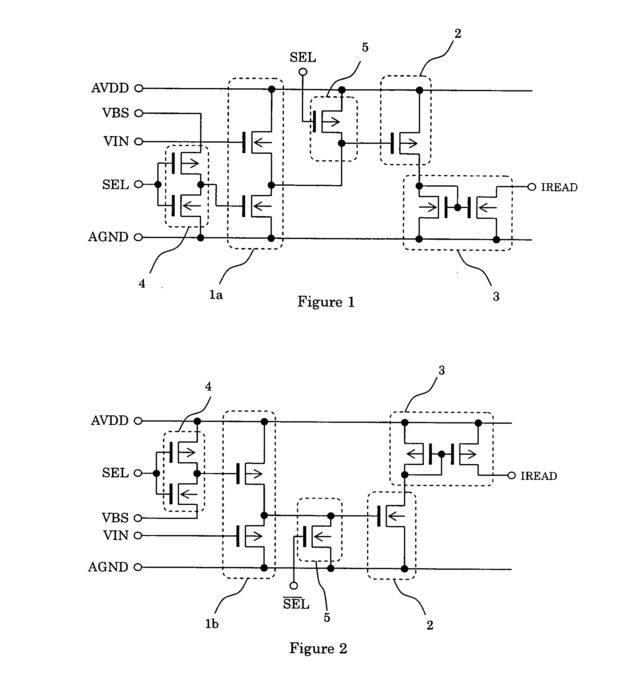
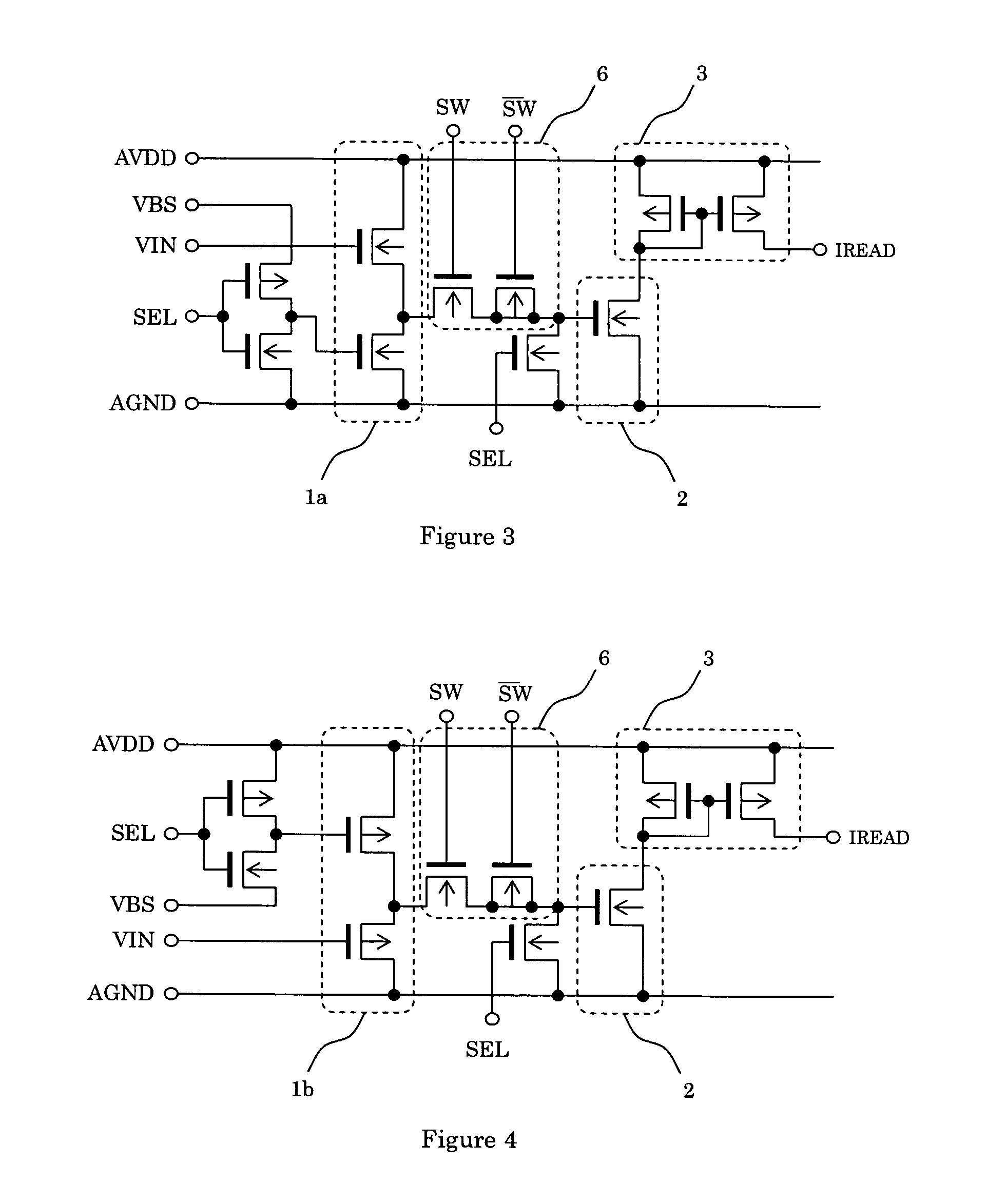
[0019]FIG. 1 shows the circuit diagram of the power supply noise measuring circuit of the present invention. The power supply noise measuring circuit of the present invention, adapted to a semiconductor integrated circuit including plural circuit blocks for conducting signal processing, comprises a n-type source follower 1a connected the input node to the power supply line to be measured, a signal conversion amplifier circuit 2 converting voltage-input to current-output which input is the output of the source follower 1a, and a current readout circuit 3 for reading out the output current of the signal conversion amplifier circuit 2. In addition, FIG. 1 shows other circuit elements of the power supply noise measuring circuit, an inverter circuit 4 having a function for activating the power supply noise measuring circuit selectively, and a cut-off switch 5 for switching the current readout circuit 2.

[0020] Hereinafter, the operation of the power supply noise measuring circuit of the ...


PUM


Abstract

A noise measuring circuit and a noise measuring circuit of the present invention can figure out power supply noise waveforms, ground level noise waveforms, and a spatial distribution of noise occurring positions by being embedded into distributed arrangement positions in said semiconductor integrated circuit comprising plural circuit block for performing a digital signal processing, and the noise measuring circuit and the noise measuring circuit is manufactured by the manufacturing process of the CMOS semiconductor integrated circuit. The power supply noise measuring circuit and the ground level noise measuring circuit comprise a source follower, a select read out switch, and source-grounded amplifier. These noise measuring circuits can be configured by several (about 6) MOS transistors, so the layout for the measuring circuit can be small and be achieved by the same size as that of a standard cell type logic gate circuit. As for the output of the noise measuring circuits, the output current of said source-grounded amplifier is connected to the current bus line, the outputted current is amplified and the amplified current is read by driving the external resistance load circuit. Plural noise measuring circuits can be connected parallel to the current bus line, and the multiple points noise measuring in the main integrated circuit can be achieved by reading out the output current.

Description

TECHNICAL FIELD [0001] The present invention relates to a noise measuring circuit for detecting and measuring noise included in the power supply signal or the ground level signal of a large-scale integrated circuit device. BACKGROUND ART [0002] Due to the progression of the large-scale design in the semiconductor device accompanying the micro-fabrication technology development in the semiconductor manufacturing process, voltage fluctuation may occur in the power supply signal or the ground level signal when the integrated circuit device is activated. The voltage fluctuation deteriorates the reliability of the integrated circuit operation. With a view to solve the above-mentioned problem, in order to analyze the malfunction which causes the error in the integrated circuit, an evaluation method for evaluating the voltage fluctuation in the power supply signal or in the ground level signal is strongly required, in short, a noise evaluation method is strongly required. [0003] Convention...

Claims


Application Information

Patent Timeline
05 Oct 2006
Publication
US20060221531A1
IPC
H02H9/06; G01R31/28; G01R31/3173; H01L27/04
CPC
G01R29/26; G01R31/3173; H01L2924/0002; H01L2924/00; G11C29/00; G11C5/14
Inventors
NAGATA, MAKOTO