Semiconductor-processing apparatus provided with self-cleaning device

a technology of self-cleaning and semiconductor processing equipment, which is applied in the direction of hollow article cleaning, fluid pressure measurement, instruments, etc., can solve the problems of increased operation cost, damage to the surface of electrodes, and defect in manufactured semiconductor circuits

Inactive Publication Date: 2006-10-12
ASM JAPAN
View PDF25 Cites 76 Cited by
  • Summary
  • Abstract
  • Description
  • Claims
  • Application Information

AI Technical Summary

Benefits of technology

[0057] Additionally, the present invention is not limited to the above-mentioned embodiments or aspects; for example, any element used in an embodiment can interchangeably be used in another embodiment, and any combination of elements can be applied in these embodiments, unless it is not feasible. Additionally, it is to be understood that no necessarily all such objects or ad...

Problems solved by technology

This causes impurity contamination that leads to defects in manufactured semiconductor circuits.
As a result, the surface of electrodes is damaged; a surface layer comes off to cause impurity contamination.
It becomes necessary to replace damaged parts frequently, which increases operation cost.
In a remote plasma cleaning method using a remote plasma chamber, however, because radio-frequency power is not applied to electrodes inside a reactor, the above-mentioned plasma emission or voltage/current information of a radio-frequency power supply line cannot be obtained.
However, because a state, an amount generated, a temperature, etc. of reaction products adhering to the reactor exhaust piping portion do not necessarily have constant correlation with those inside the reactor, accurate information of the interior of the reactor cannot be detected by the above-mentioned cleaning endpoint detection device installed in the reactor exhaust piping por...

Method used


Image

  • Semiconductor-processing apparatus provided with self-cleaning device
  • Semiconductor-processing apparatus provided with self-cleaning device
  • Semiconductor-processing apparatus provided with self-cleaning device

Examples


embodiments

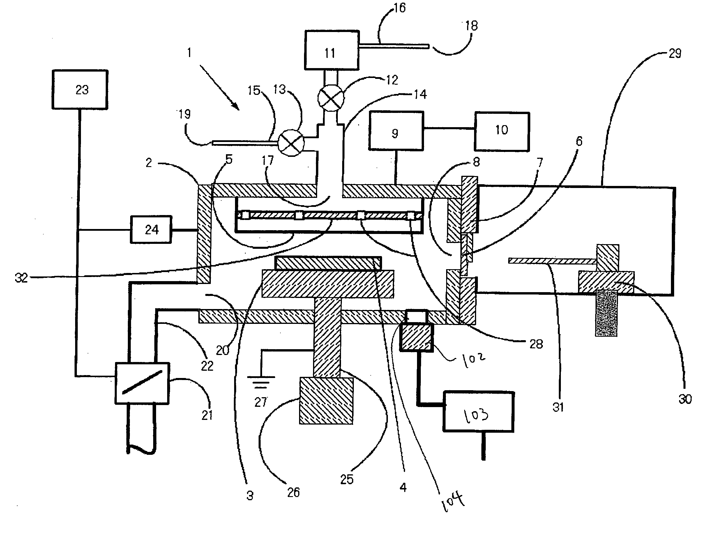
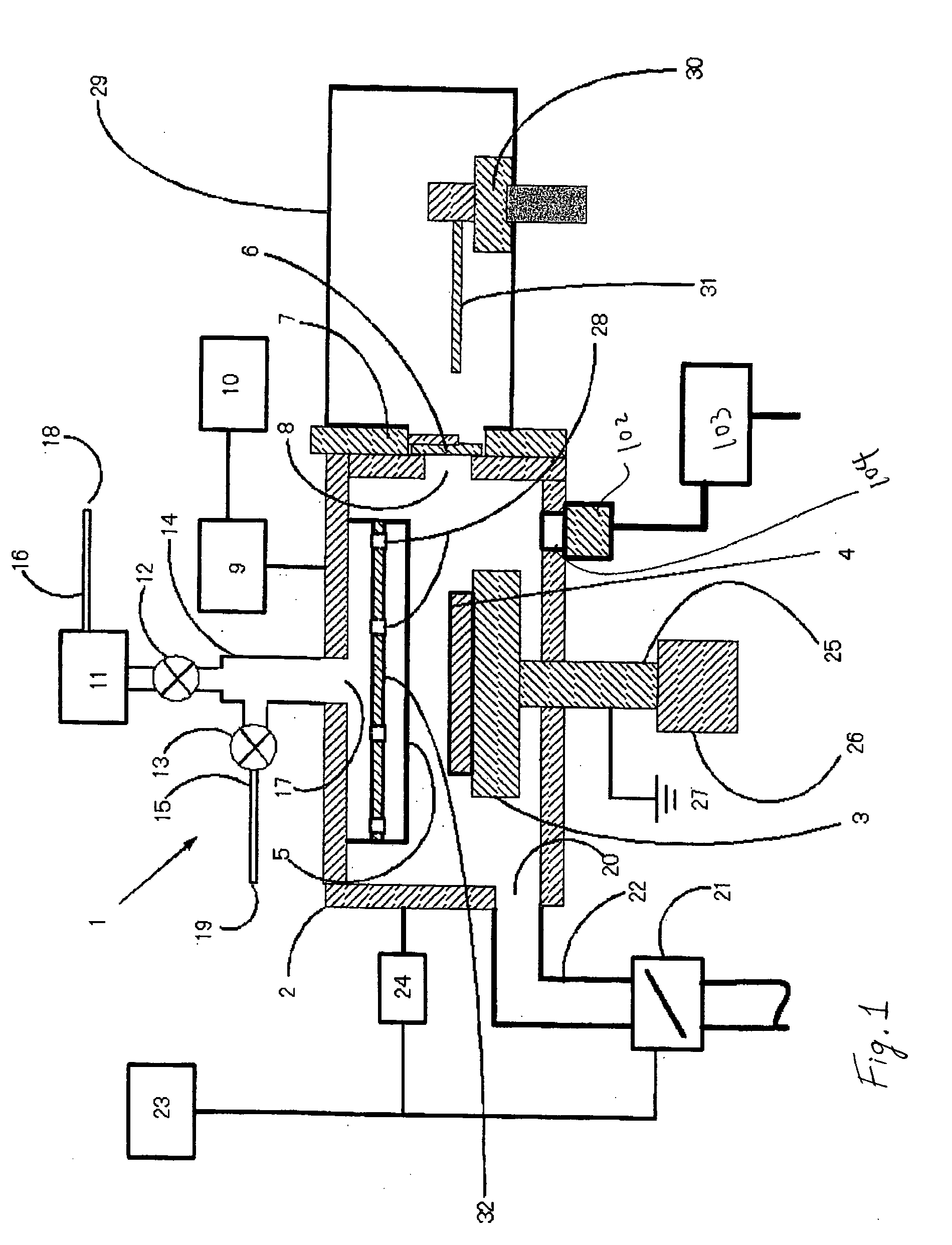
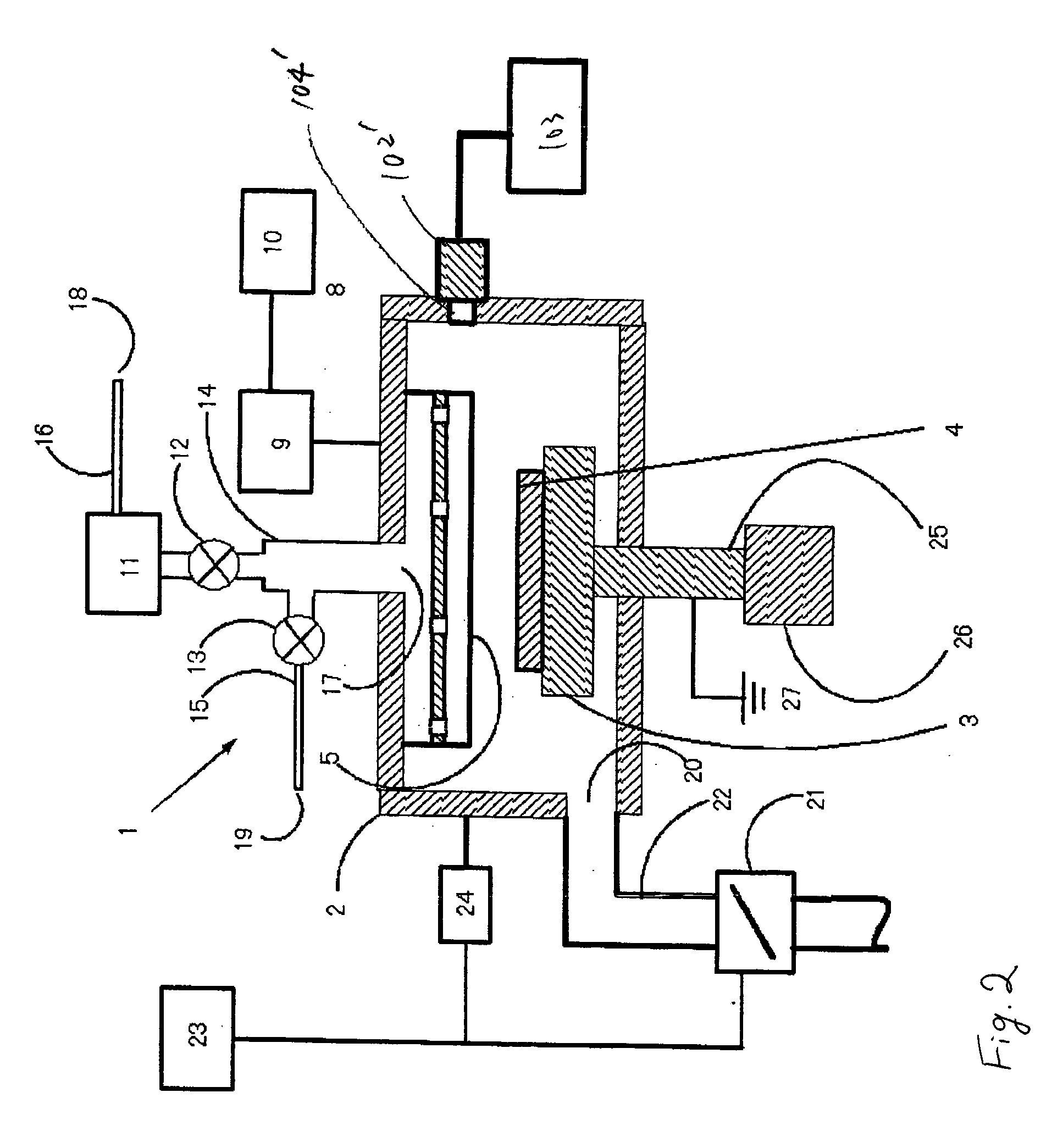
[0115] Film formation was executed using a CVD apparatus shown in FIG. 1. 250 sccm of TEOS (250 cc per 1 min, 0° C., 1 atm) and 2,300 sccm of oxygen were supplied into a reactor 2; while maintaining a pressure inside the reactor 2 at 400 Pa, by applying 13.56 MHz radio-frequency power at 650 W and 430 kHz radio-frequency power at 500 W to the showerhead 5, a plasma discharge zone was formed between the susceptor on which a φ300 mm silicon wafer is placed and the showerhead 5. As a result, in 40 sec., a 500 nm thick silicon oxide film having uniformity ±1.5% (a value obtained by measuring a film thickness of a 500 nm thick silicon oxide film grown on the silicon wafer at 49 points and dividing a difference between the maximum value and the minimum value of measured values by ½ of an average value of all measured values and expressing it in percentage) was able to be formed on the silicon wafer.

[0116] Upon completion of a thin film formation process, the valve 13 was closed and simul...


PUM


Abstract

A CVD apparatus comprising an optical unit detecting the mass of contaminants adhering to an inner surface of a CVD reactor by irradiating an inner surface of the reactor with light having monochromaticity through an optical window provided on an inner wall of the reactor and receiving its reflected light is provided.

Description

BACKGROUND OF THE INVENTION [0001] 1. Field of the Invention [0002] The present invention relates to a semiconductor-processing apparatus with a self-cleaning device; particularly to a plasma CVD apparatus with a self-cleaning device comprising a cleaning endpoint detection device. [0003] 2. Description of the Related Art [0004] CVD apparatuses have been conventionally used to form insulation films such as silicon oxide, silicon nitride, amorphous carbon or polymer containing benzene ring, conductor films such as tungsten silicide, titanium nitride or aluminum alloy, and high-dielectric films containing PZT(PbZr1-xTixO3) or BST(BaxSr1-xTiO3) on a silicon substrate or a glass substrate. [0005] In order to form these films, reaction gas having various compositions or a second reaction gas is supplied into a reactor. These gases cause a chemical reaction by receiving plasma energy, and a desired thin film is formed on a semiconductor substrate. Inside the reactor, a film generated simi...

Claims


Application Information

Patent Timeline
IPC IPC(8): C23C16/00B08B6/00H01L21/00B05C11/00
CPCB08B7/0035C23C16/52C23C16/4405
Inventor SATOH, KIYOSHIKANO, YOSHINOBU
Owner ASM JAPAN
Why Eureka
Try Eureka