
Field effect transistor and method for fabricating it

Inactive Publication Date: 2006-10-19
INFINEON TECH AG
View PDF17 Cites 10 Cited by
  • Summary
  • Abstract
  • Description
  • Claims
  • Application Information

AI Technical Summary

Benefits of technology

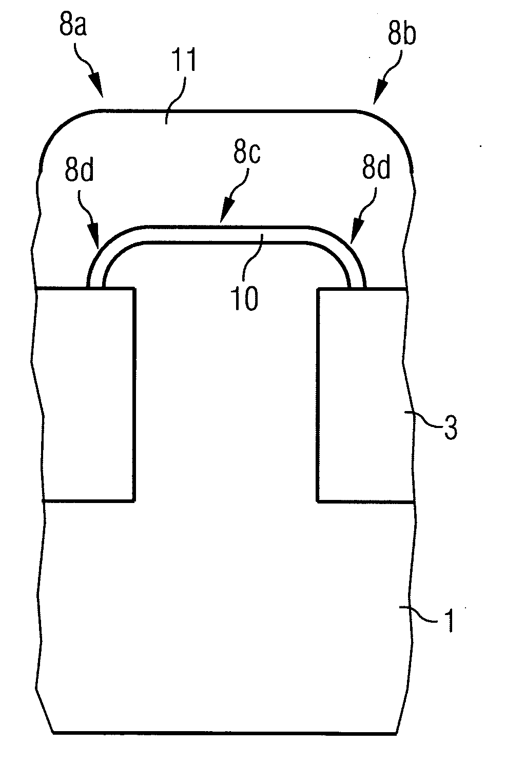
[0024] The field-effect transistor according to the invention has the advantage that it is possible to ensure a significant increase in the effective channel width for the forward current ION compared with previously used, conventional transistor structures, without having to accept a reduction of the integration density that can be attained. Thus, by way of example, the forward current ION can be increased by up to 50%, without having to alter the arrangement of the active regions or of the trench isolation. The transistor according to the invention advantageously utilizes a part of the area which, in conventional transistors, is provided for the isolation between the transistors. In this case, the channel width can be enlarged in a self-aligned manner without the risk of short circuits.
[0027] The field-effect transistor according to the invention furthermore has the advantage that the “corner” effect brought about geometrically in conventional transistors, on account of field-induced local electron accumulation, can be largely avoided. Furthermore, in the case of the field-effect transistor according to the invention, it is possible to dispense with the previous strong topology between the trench isolation and the channel region. The field-effect transistor according to the invention or the method according to the invention furthermore has the advantage that it can be integrated into different semiconductor technologies (e.g. logic or memory) without a high outlay.
[0033] In accordance with a further preferred embodiment of the method according to the invention, before the production of the gate oxide, a sacrificial oxide is applied, which is subsequently removed again. The use of a sacrificial oxide results in very good through-oxidation of the interface between the part of the channel region that covers the trench isolation and the trench isolation, which is preferably filled with oxide.

Problems solved by technology

The characteristic parameters of conventional field-effect transistors, in particular of planar MIS field-effect transistors (MISFET), are increasingly impaired with continual structural miniaturization (scaling) and increasing of the packing density of integrated circuits.
Despite all these measures, however, it is becoming more and more difficult to ensure an adequate forward current ION above a feature size of about 100 nm, without the risk of tunnelling or degradation of the gate oxide stability of the MISFET.
Unfortunately, all of the measures mentioned either have only limited efficacy or they require a high process engineering outlay.

Method used


Image

  • Field effect transistor and method for fabricating it
  • Field effect transistor and method for fabricating it
  • Field effect transistor and method for fabricating it

Examples


Embodiment Construction

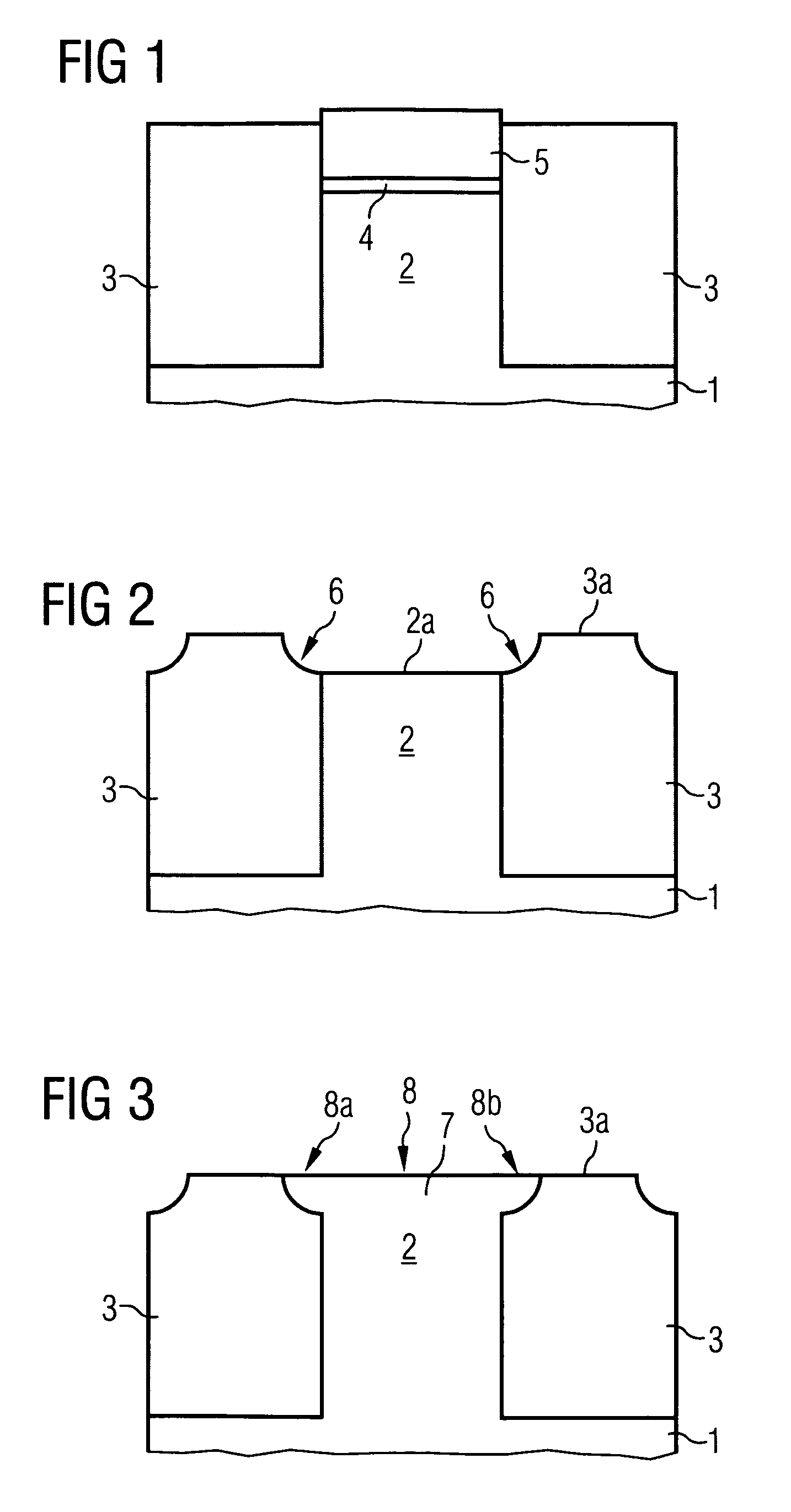
[0045] FIGS. 1 to 3 show a first embodiment of the method according to the invention for fabricating a field-effect transistor. The starting point of the method according to the invention is a semiconductor substrate 1, for example a silicon substrate, which has active regions 2 and an already completed trench isolation 3 between the active regions 2. For reasons of clarity, only one active region is shown of the many active regions which are typically present in the semiconductor substrate 1. The field-effect transistor is produced hereinafter in the region of the active region.

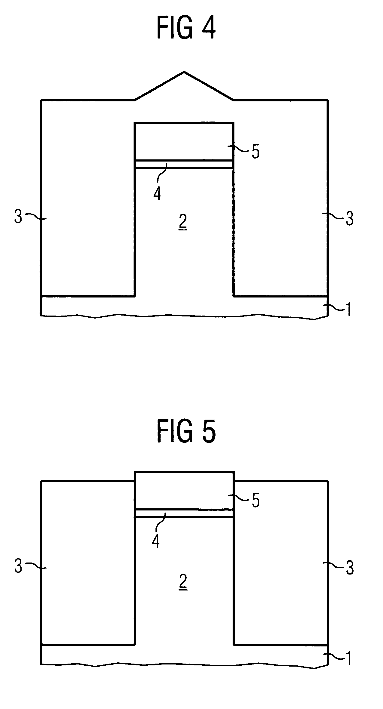
[0046] A pad oxide layer 4 and a pad nitride layer 5 are arranged above the active region. These layers were used inter alia to produce the trench isolation 3. The trench isolation 3 is obtained for example by filling a trench that has been etched into the semiconductor substrate 1 with silicon oxide with the aid of an HDP method (“high density plasma”). In this case, a so-called “liner”, for example a nitr...


PUM


Abstract

A transistor is provided which advantageously utilizes a part of the area which, in conventional transistors, is provided for the isolation between the transistors. In this case, the channel width can be enlarged in a self-aligned manner without the risk of short circuits. The field-effect transistor according to the invention has the advantage that it is possible to ensure a significant increase in the effective channel width for the forward current ION compared with previously used, conventional transistor structures, without having to accept a reduction of the integration density that can be attained. Thus, by way of example, the forward current ION can be increased by up to 50%, without having to alter the arrangement of the active regions or of the trench isolation.

Description

CLAIM FOR PRIORITY [0001] This application claims priority to PCT / EP02 / 06-803, filed in the German language on Jun. 19, 2002, which claims the benefit to German Application No. DE 101 31237.7, filed in the German language on Jun. 28, 2001. TECHINCAL FIELD OF THE INVENTION [0002] The present invention relates to a field-effect transistor and a method for fabricating it. BACKGROUND OF THE INVENTION [0003] The characteristic parameters of conventional field-effect transistors, in particular of planar MIS field-effect transistors (MISFET), are increasingly impaired with continual structural miniaturization (scaling) and increasing of the packing density of integrated circuits. Thus, by way of example, with a shortened channel length of the transistor the threshold voltage VT of the transistor decreases. At the same time, with a shortened channel length, the field strength in the channel region and the reverse current IOFF increase (SCE: short channel effect; roll-off). Furthermore, with...

Claims


Application Information

Patent Timeline
IPC IPC(8): H01L29/76H01L29/94H01L21/8234H01L21/336H01L31/00H01L29/78H01L21/762H01L29/06
CPCH01L21/76229H01L21/823481H01L29/7851H01L29/66651H01L29/0653H01L29/772
Inventor POPP, MARTINRICHTER, FRANKTEMMLER, DIETMARWICH-GLASEN, ANDREAS
Owner INFINEON TECH AG
Learn More