Low voltage flexible organic/transparent transistor for selective gas sensing, photodetecting and CMOS device applications

a flexible organic/transparent transistor, selective gas sensing technology, applied in the field of thin film transistors, can solve the problems of low manufacturing cost, operating voltage, between 10 and 100 v, of tfts with low-k gate dielectrics on plastic substrates that are commonly too high

Inactive Publication Date: 2006-10-19
MASSACHUSETTS INST OF TECH
View PDF10 Cites 3941 Cited by
  • Summary
  • Abstract
  • Description
  • Claims
  • Application Information

AI Technical Summary

Benefits of technology

[0008] According to one aspect of the invention, there is provided a thin film transistor (TFT). The TFT includes a source electrode, a drain electrode, and a gate electrode. A gate dielectric is coupled to the source electrode, drain electrode, and gate electrode. The gate insulator includes room temperature deposited high-K materials so as to allow said thin film transistor to operate at low voltage.
[0009] According to another aspect of the invention, there is provided a method of forming a thin film transistor (TFT). The method includes forming a source electrode, a drain electrode, and a gate electrode. Also, the method includes forming a gate dielectric that is coupled to the source electrode, drain electrode, and gate electrode. The gate insulator includes room temperature deposited high-K materials so as to allow said thin film transistor to operate at low operating voltage.

Problems solved by technology

Advantages of TFT-based sensors include high sensitivity and selectivity, resulting from special features of organics e.g. their specialized bonding sites, coupled with the ability to use flexible substrates and low temperature processing leading to low manufacturing costs.
While this can be done in principle with other types of sensors such as SAW (surface acoustic wave) devices, quartz crystal microbalances (QCM), organic / inorganic resistors, their size and complexity often make this impractical.
To date, the operating voltages, between 10 and 100 V, of TFTs with low-K gate dielectrics on plastic substrate are commonly too high, especially for portable, battery-powered sensing device applications, e.g. medical monitoring and / or toxic chemical sensors integrated within military uniforms.

Method used


Image

  • Low voltage flexible organic/transparent transistor for selective gas sensing, photodetecting and CMOS device applications
  • Low voltage flexible organic/transparent transistor for selective gas sensing, photodetecting and CMOS device applications
  • Low voltage flexible organic/transparent transistor for selective gas sensing, photodetecting and CMOS device applications

Examples


Embodiment Construction

[0015] By introducing High-K gate dielectrics, one can successfully reduce the operating voltages for TFTs sensors, photodetectors, and CMOS circuits. The invention utilizes the high K-dielectric Bi1.5Zn1.0Nb1.5O7 (BZN series, A2B2O7 pyrochlore structure materials) with relative dielectric constants of 50-55 depending on growth method. High-K BZN films can be deposited by sputtering, pulsed laser deposition, chemical vapor deposition method, spray drying with nano-particle incorporation, printing techniques, or other techniques.

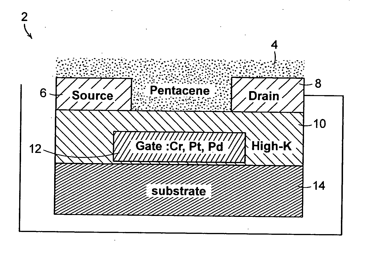
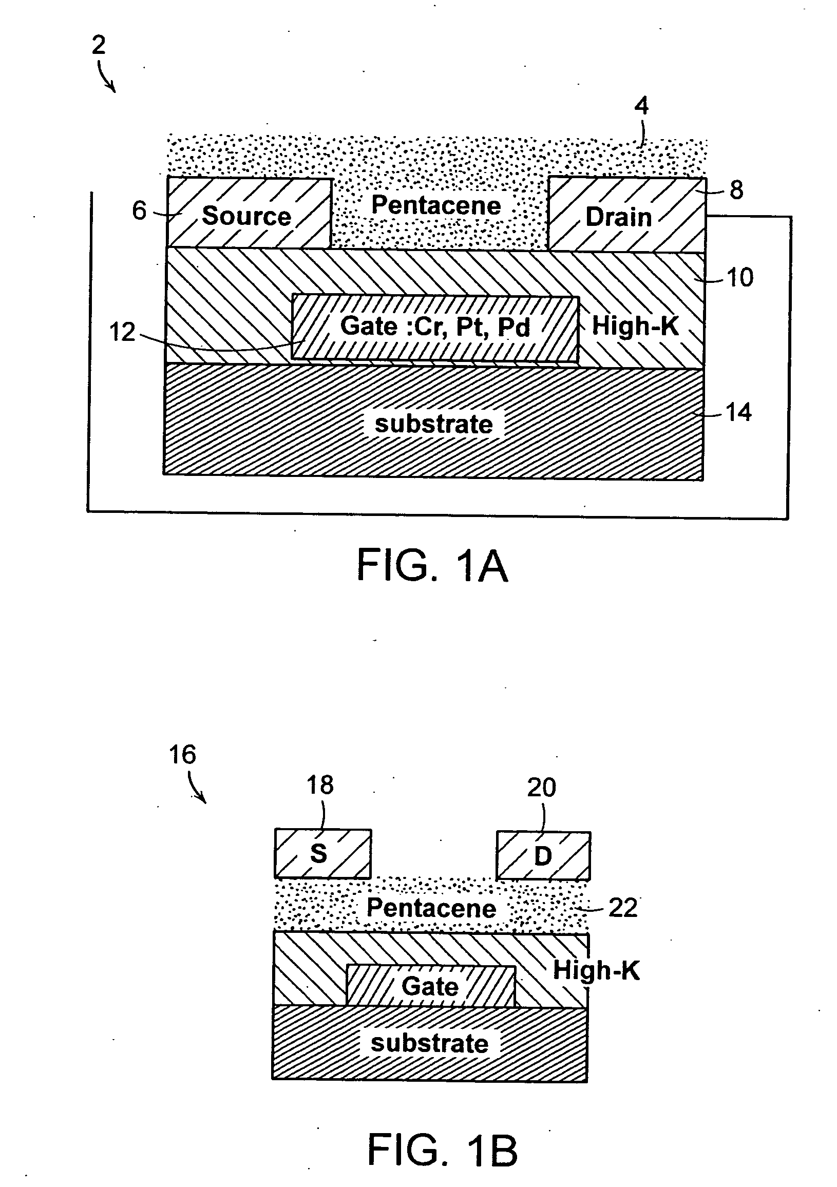
[0016] The invention provides an environment for which both organic and inorganic transistors having high-K gate dielectrics can be used. First, the organic thin film transistor (OTFT) includes a semiconductor layer comprising pentacene, however in other embodiments, conjugated polymers such as poly-3-alkykthiophene, poly-3-hexylthiophene (P3HT), poly-thienlylene vinylene or tetracene can be used as the semiconductor layer. FIGS. 1A-1B are schematic diagrams...


PUM

PropertyMeasurementUnit
operating voltagesaaaaaaaaaa
voltageaaaaaaaaaa

Abstract

A thin film transistor (TFT) includes a source electrode, a drain electrode, and a gate electrode. A gate insulator is coupled to the source electrode, drain electrode, and gate electrode. The gate insulator includes room temperature deposited high-K materials so as to allow said thin film transistor to operate at low operating voltage.

Description

PRIORITY INFORMATION [0001] This application claims priority from provisional application Ser. No. 60 / 665,751 filed Mar. 28, 2005, which is incorporated herein by reference in its entirety.BACKGROUND OF THE INVENTION [0002] The invention relates to the field of transistors, and in particular to a thin film transistor (TFT) having high-K gate dielectrics. [0003] Thin film transistor (TFT) technology on plastic substrates offers many potential advantages not only with respect to displays but also to wide area digital logic circuitry, electronic-paper and books, wearable electronics, sensors, photodetectors, actuators. Room temperature fabricated Organic-TFTs (OTFTs) and ZnO-based transparent-TFTs can contribute to reduced cost by substituting inexpensive plastic substrates for relatively high cost Si wafers or flat glass substrates utilized today. [0004] TFT-type sensors are undoubtedly of great importance for the development of microelectronics-based smart sensing systems. Several pa...

Claims


Application Information

Patent Timeline
Patent Type & Authority Applications(United States)
IPC IPC(8): H01L29/94
CPCH01L21/31691H01L27/14643H01L27/305H01L29/4908H01L29/7869H01L51/0036G01N27/4141H01L51/0097H01L51/0525H01L51/0529H01L51/0545H01L51/428Y02E10/549H01L51/0052H01L21/02266H01L21/02197H01L21/02269H01L21/0228H10K39/30H10K85/113H10K85/615H10K10/472H10K10/474H10K10/466H10K30/65H10K77/111
Inventor KIM, IL-DOOTULLER, HARRY L.
Owner MASSACHUSETTS INST OF TECH
Why Eureka
Try Eureka