

Standard member for length measurement, method for producing the same, and electron beam length measuring device using the same
a technology of length measurement and standard member, which is applied in the direction of material analysis using wave/particle radiation, instruments, calibration apparatus, etc., can solve the problems of measurement difficulty, diffraction angle measurement of diffraction grating using laser light used for calibration, and measurement limitation, etc., to achieve excellent resolution, improve uniformity within a sample surface, and improve accuracy. the effect of calibration
- Summary
- Abstract
- Description
- Claims
- Application Information
AI Technical Summary
Benefits of technology
Problems solved by technology
Method used
Image

Examples
Embodiment Construction
[0043] Hereafter, embodiments of this invention will be described with reference to the drawings.
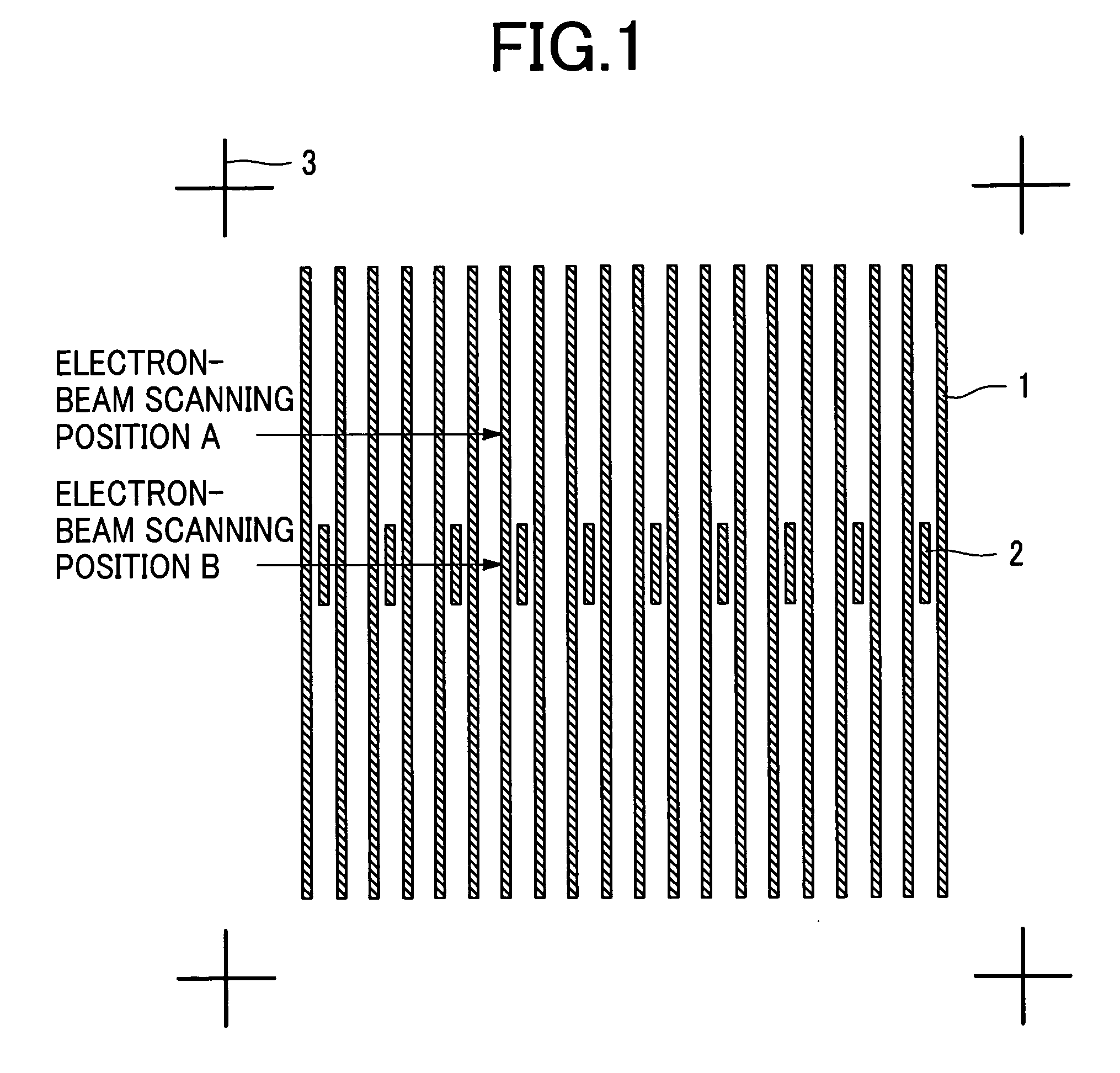
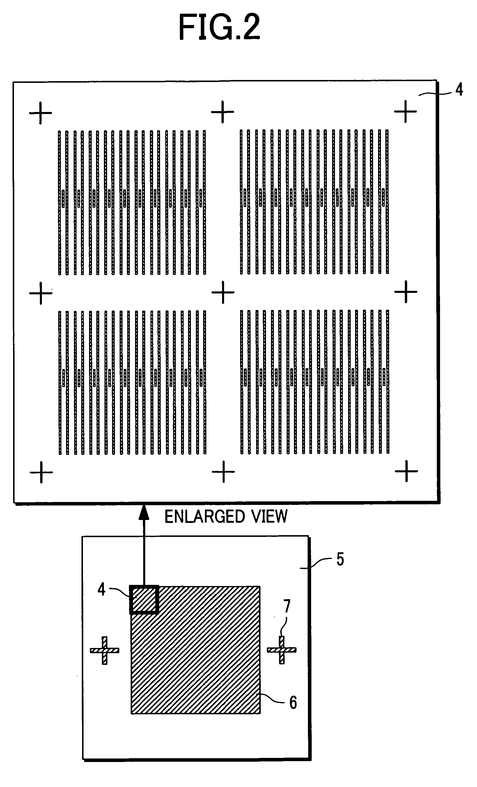
[0044] An example of a dimension standard component for an electron-beam metrology system of this invention is shown in FIG. 1 and FIG. 2. FIG. 3 shows the conventional dimension standard component for the electron-beam metrology system.
[0045] Conventionally, a depression-and-projection pattern 15 on a semiconductor substrate of the (110) plane (for example, a silicon (Si) substrate, a compound semiconductor substrate, such as of GaAs and InP) has been fabricated by laser interferometer lithography method and wet chemical etching as a diffraction grating pattern in a fixed direction as shown in FIG. 3. The pitch dimension of the diffraction grating 9 is about 200 nm; this value has been found by the diffraction angle measurement using a laser. The pattern is uniformly formed all over the sample surface 8 of 4-mm square. In the case where the electron-beam metrology system is calibrated...
PUM
| Property | Measurement | Unit |
|---|---|---|
| wavelength | aaaaa | aaaaa |
| wavelength | aaaaa | aaaaa |
| length measurement | aaaaa | aaaaa |
Abstract
Description
Claims
Application Information