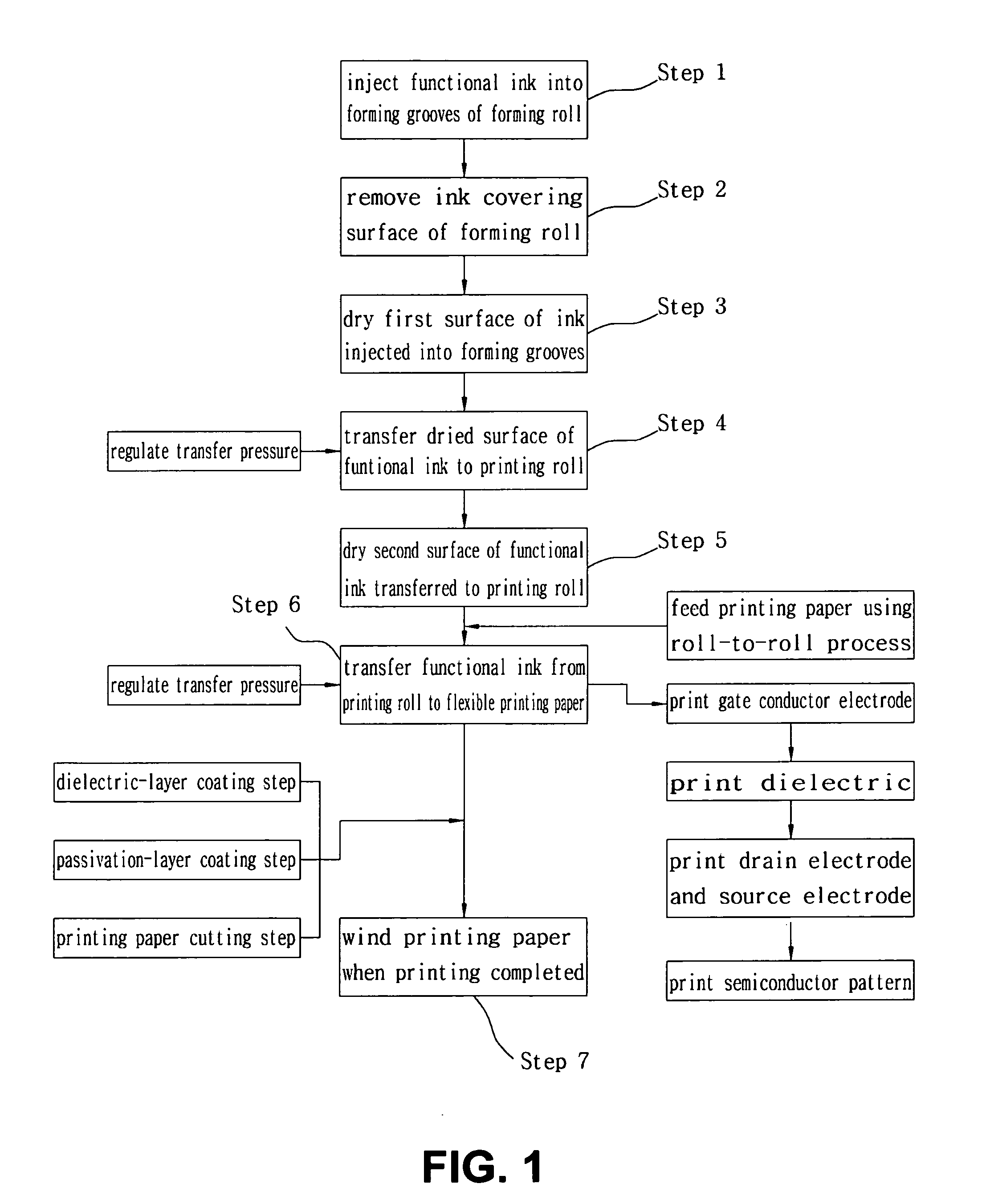
Thus, an important
deposition process, such as a
sputtering process, is performed under high temperature and vacuum conditions, using expensive precision equipment.. Most manufacturing and inspecting operations require a very
clean environment.
In this case, manufacturing costs will further increase.
Meanwhile, the production of an IC
chip which has a low grade, that is, a kilo-grade, has low economic efficiency.
Thus, even if the kilo-grade chip is required, it will not be produced.
When new-generation RFID / USN electronic devices, which are most electronic devices for general purposes, are manufactured using current
silicone semiconductor technology, manufacturing costs are high.
Thus, it is impossible to supply the electronic devices at low cost.
However, the production of the IC chip is not easily realized through the printing method using various kinds of functional ink.
First, the IC chip cannot be produced through printing because of an ink material.
Inventive ink material is still in an initial development stage with respect to characteristics, durability, and cost, so that it is unfeasible to use the ink material in practice.
That is, the quality of the ink material and production technology therefor are insufficient, so that the ink material cannot be
mass-produced.
Further, if a printer, which is the important element for producing a printed IC chip, is not modified to be suitable for manufacturing IC chips but is a general printer for printing
graphics or images, it is impossible to develop or produce a micro printed IC chip as desired.
However, if a print having a finer pattern is required, it is impossible to manufacture a desired electronic device using the general screen printer.
However, the resolution of the equipment has not reached the resolution required for manufacturing IC chips.
No matter how the precision screen printer or the stencil printer is developed to be generally used for producing electronic devices, it does not overcome the limitation of the stage production process.
However, unless a new rotary pressing technology and a new ink transfer method for a printed IC chip, which must be fundamentally superior to existing image information printing technology and printers optimized for a person's
visual discrimination, are developed, a conventional rotary press cannot be utilized.
In order to perform even a printing test of a conventional printer, a person must master a complicated plate-making operation and a difficult multi-stage control operation for driving the printer.
However, the ink jet printing method basically uses dot printing technology, unlike other printing methods.
Thus, several problems may occur in the application of the ink jet printing method to line pattern printing.
In a detailed description, the ink jet printing method is disadvantageous compared to a typical printing method which is performed in a contact manner using a printing plate, in consideration of a pin hole forming a line using dots, gaps,
surface roughness, edge roughness, difficulty in forming lines of various widths, and positional misalignment when repeatedly printing.
Further, in the case where
mass production is attempted, the movement of many nozzles when a plurality of engine sets comprising a great number of ink jet heads is moved is complicated in comparison with a very simple printing using a printing plate.
Hence, it is difficult to obtain uniform print quality, especially when micro printing.
However, the technology making a silicone-rubber printing plate having a fine pattern corresponding to a sub micro grade using advanced silicone
semiconductor technology, and realizing the pattern of a fine
corrosion-preventing film using SAM ink, which is an expensive high-grade material, is used only for producing expensive IC chips.
Therefore, the
soft lithography printing method is not printing technology suitable for efficiently producing a printed IC chip that is inexpensive and has a simple function.
However, it may only substitute for
photoresist patterning in the silicone semiconductor process, and is only useful as a batch printing method for a substrate having a larger area.
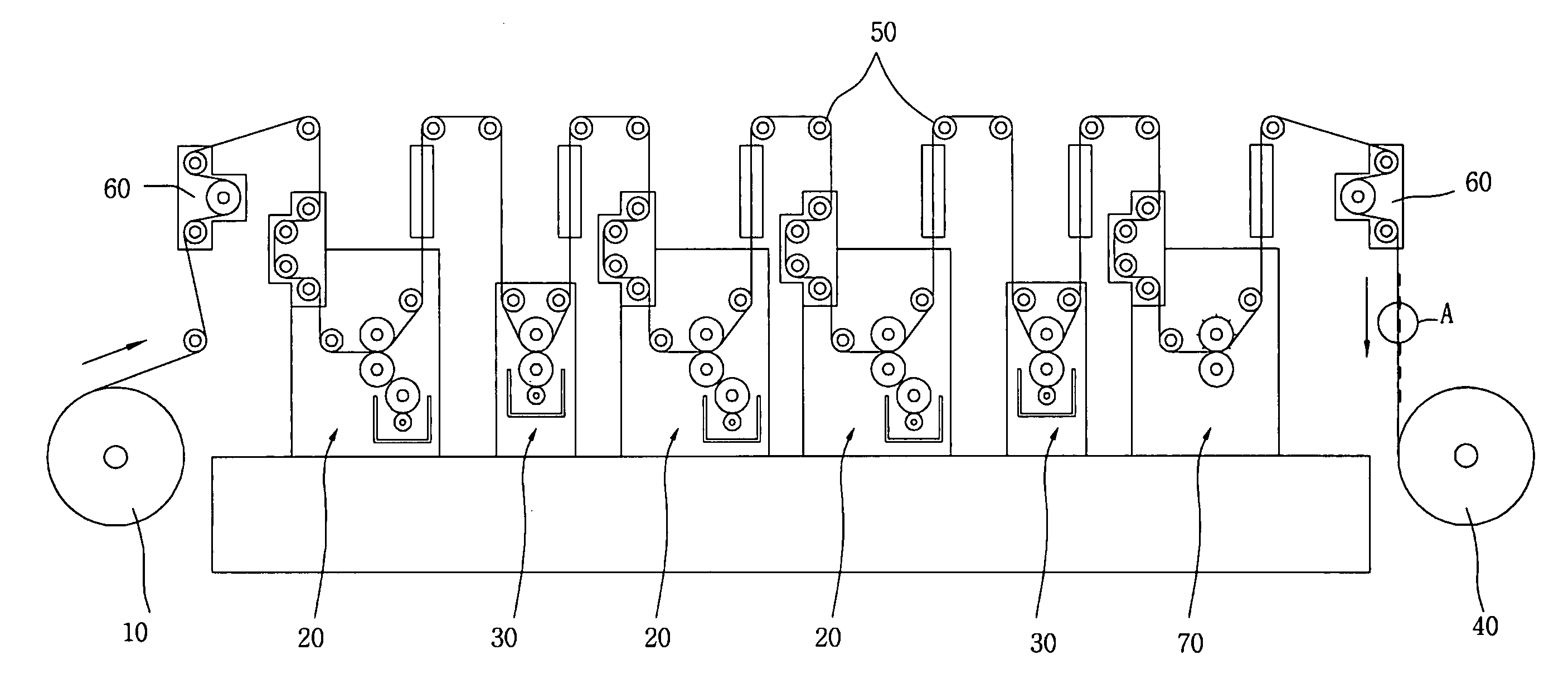
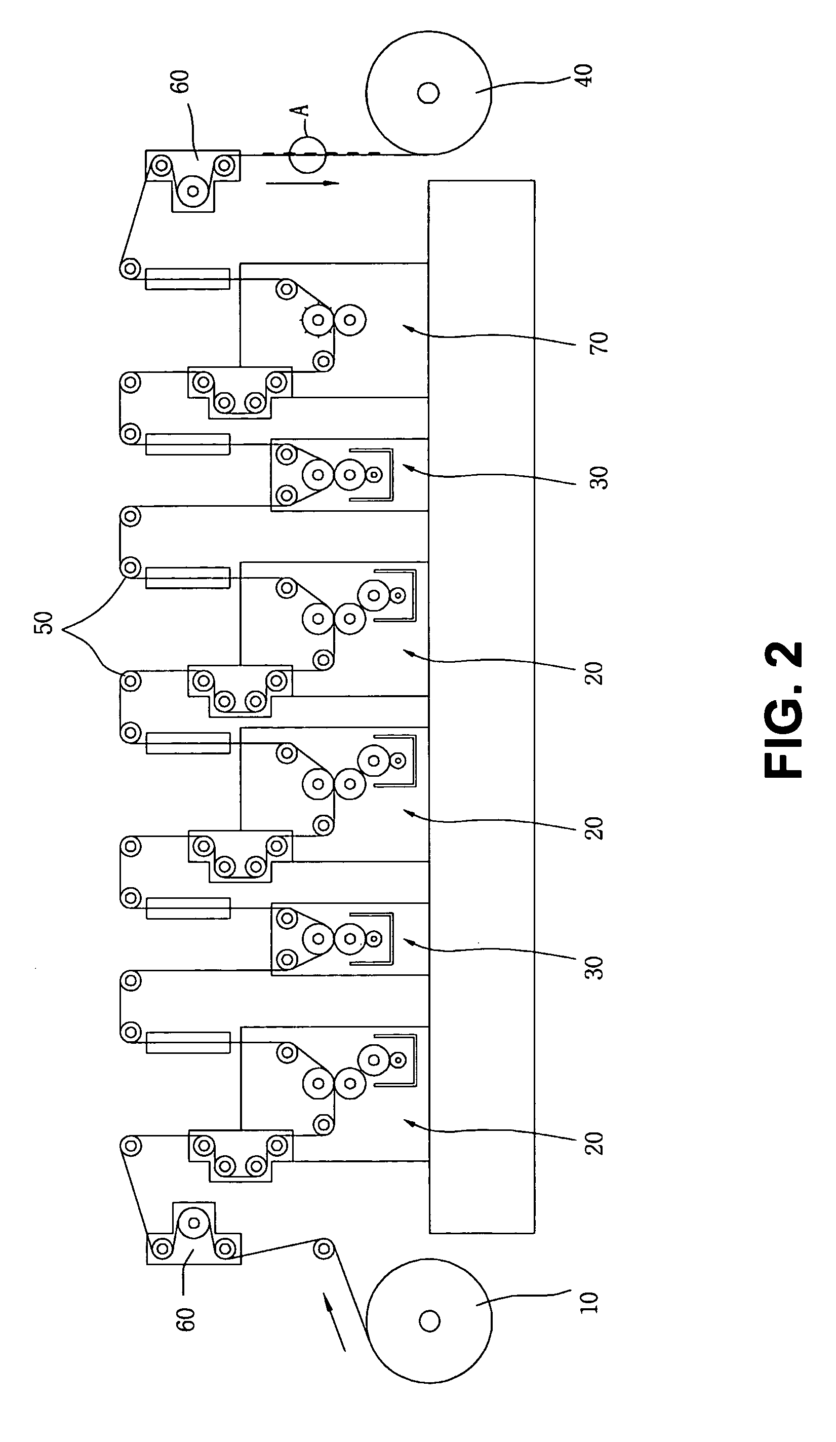
That is, according to the prior art, a shaft and gears are complicatedly mechanically coupled to one main motor, thus rotating many cylinders of respective units.
Further, the ink supply amount is automatically controlled by
vision control employing a
digital camera, and the drive cylinder of each printing unit is delicately controlled with respect to the rotating direction and the axial direction for the purpose of precise registration.
However, the current rotary press for printing newspaper cannot be used to print an IC chip.
However, since the current printing technology is set to 100 μm, the technology cannot be applied to print and produce an IC chip requiring a design rule of 10 μm.
However, the line pattern of the printed IC chip does not tolerate the above-mentioned printing defects, but strictly requires the printing of a pattern and shape having reliable physical parameters.
That is, printing which produces a line-
gain beyond an allowable tolerance, in addition to having the problems of pin holes, discontinuities, roughness, etc., is unacceptable.
Further, printing
layers printed one by one must be neatly transferred, the physical properties of overlapping printing
layers must not be mixed with each other, and insufficient
drying, leading to intermixing, is unacceptable.
However, when an IC chip is produced through a roll-to-roll rotary pressing process, desired productivity and economical efficiency cannot be achieved unless real-time inspection is conducted through a non-
contact type of in-line
inspection method, as in general printing.

