Fast hopping frequency synthesizer using an all digital phased locked loop (ADPLL)

a phase locked loop and frequency synthesizer technology, applied in the field of data communication, can solve the problems of long settling time, inability to construct a single phase locked loop with reasonable phase noise, and need to be a pll running continuously, etc., and achieve the effect of small size ic area and low power consumption

Active Publication Date: 2006-11-16
TEXAS INSTR INC
View PDF8 Cites 41 Cited by
  • Summary
  • Abstract
  • Description
  • Claims
  • Application Information

AI Technical Summary

Benefits of technology

[0023] A key feature of the present invention is that unlike the prior art, a single DCO is used to implement a UWB compliant transmitter that meets the UWB specifications of avoiding excessive frequency spurs outside the bands of interest. Use of DCO controlled by an ADPLL by the frequency synthesizer of the present invention eliminates the need for both simultaneous generation of all local oscillator (LO) signals as well as modulation of multiple synthesizers.
[0024] Several advantages of the present invention include (1) only a single DCO is required which operates in an open-loop mode, (2) the resulting spectrum is very quiet at the LO frequencies (i.e. free of spurs), (3) exhibits very low power consumption, (4) requires a significantly smaller size IC area, and (5) provides a self-calibration process that selects accurate OTWs thus insuring FCC and UWB specifications are met.

Problems solved by technology

The underlying trade off is that lower loop bandwidths may provide lower phase noise by better rejecting the reference phase noise but at a cost of longer settling times.
It is appreciated by one skilled in the art that a single phase locked loop with reasonable phase noise and a settling time of 9 ns is impractical to construct using conventional means.
A major drawback of this architecture is that for each possible frequency there needs to be a PLL running continuously.
This requires a large area (i.e. in either board size or die area) with a consequent large power dissipation.
Further, a large enough frequency set may make this scheme impractical to construct.
Although this prior art architecture generally requires a smaller number of PLL circuits than the architecture shown in FIG. 3, the configurable mixer stage usually generates (aside from the desired LO tone) a number of spurious tones which degrade the Spectral Emission Mask (SEM) in the transmitter and pick up (i.e. demodulate into the same frequency band) undesired signals in the receiver.
A major disadvantage of this architecture is that although the circuit reduces the number of PLL circuits required, with a reduction in area and power count, the SSB mixer 102, along with the desired LO signal, generates a frequency comb at frequencies of 3960 MHz ±n528 MHz, where n is an integer.
This results in both spurious emissions in neighboring UWB bands in the transmitter and reduced Adjacent Channel Interferer (ACI) performance in the receiver.
Although this receiver architecture does not suffer from the spurious tone effects as does the architecture of FIG. 5, it does require three PLL circuits and three down conversion mixer pairs creating a significant size and power dissipation penalty.

Method used


Image

  • Fast hopping frequency synthesizer using an all digital phased locked loop (ADPLL)
  • Fast hopping frequency synthesizer using an all digital phased locked loop (ADPLL)
  • Fast hopping frequency synthesizer using an all digital phased locked loop (ADPLL)

Examples


first embodiment

Direct Conversion Transmitter

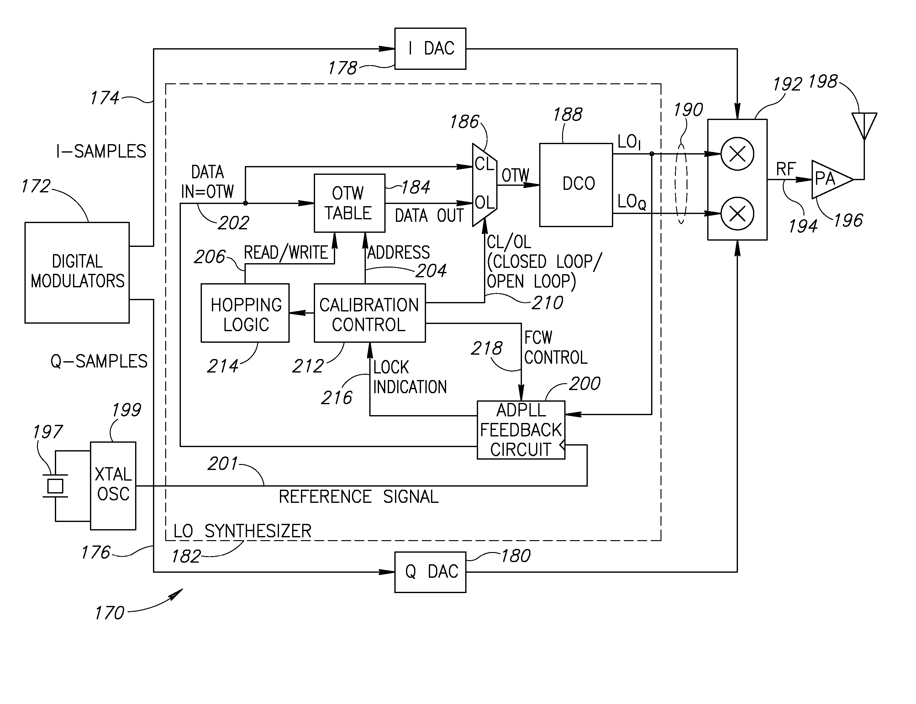
[0061] A block diagram illustrating a high-level direct conversion transmitter constructed in accordance with a first embodiment of the present invention is shown in FIG. 7. A crystal oscillator 199, coupled to a crystal 197 generates a reference signal 201. The transmitter circuit, generally referenced 170, comprises a digital modulator 172, I DAC 178, Q DAC 180, LO frequency synthesizer 182, I / Q mixer 192, power amplifier (PA) 196 and antenna 198. The frequency synthesizer 182 comprises a Digitally Controlled Oscillator (DCO) 188 coupled through an All Digital Phase Locked Loop (ADPLL) feedback circuit 200, hopping logic 214, calibration control 212, oscillator tuning word (OTW) table 184 and multiplexer 186 for opening the loop. Timing for the ADPLL feedback circuit is provided by the reference signal 201 output from the crystal oscillator 199 coupled to crystal 197. To prevent and frequency perturbations, the OTW input to the DCO is required to be ch...

second embodiment

Direct Conversion Transmitter

[0074] A block diagram illustrating a high-level direct conversion transmitter constructed in accordance with a second embodiment of the present invention is shown in FIG. 11. This second embodiment is constructed and operates similarly to that of the first preferred embodiment shown in FIG. 7 with the main difference being the introduction in the second embodiment of a mechanism to improve frequency accuracy.

[0075] The transmitter circuit, generally referenced 250, comprises a crystal oscillator 275, coupled to a crystal 273, for generating a reference signal 277, digital modulator 251, numerically controlled oscillator (NCO) 254, I DAC 264, Q DAC 265, LO frequency synthesizer 298, I / Q mixer 280, coupling circuit 284, power amplifier (PA) 286 and antenna 288. The frequency synthesizer 298 comprises a Digitally Controlled Oscillator (DCO) 276 coupled through the feedback circuit portion 296 of an All Digital Phase Locked Loop (ADPLL) (the timing for whi...

third embodiment

Direct Conversion Receiver

[0088] A block diagram illustrating a high-level direct conversion receiver constructed in accordance with a third embodiment of the present invention is shown in FIG. 15. The receiver, generally referenced 400, comprises an antenna 401, low noise amplifier 402, quadrature mixer 404, low pass filters (LPFs) 406, 408, baseband amplifiers 410, 412, analog to digital converters (ADCs) 414, 416, digital demodulator 418, crystal 420, crystal oscillator 422 and LO synthesizer 424.

[0089] In operation, the signal from the antenna is amplified by the LNA. The quadrature mixer functions to mix the amplified signal with the in phase (I) and quadrature (Q) LO signal pair 428. The resultant I baseband signal 430 and Q baseband signal 432 undergo anti-aliasing baseband filtering using analog low pass filters 406 and 408, respectively. The filter outputs undergo amplification in the baseband via amplifiers 410 and 412 and are subsequently sampled using analog to digital ...


PUM


Abstract

A novel and useful fast hopping frequency synthesizer and transmitter associated therewith. The frequency synthesizer and transmitter incorporates a digitally controlled oscillator (DCO) adapted to operate open loop. Instantaneous frequency switching is achieved by changing an oscillator tuning word (OTW) to imitate the three oscillators of a UWB transmitter. In one embodiment, the DCO can change the frequency instantaneously within the 1/fT of the varactor devices used to construct the DCO. An all digital phase lock loop (ADPLL) is used for offline calibration prior to the start of packet transmission or reception. Any phase shift during the switching is tracked by a digital circuit in the transmitter. In a second embodiment, additional frequency accuracy is provided by use of a numerically controlled oscillator (NCO) that functions to generate a fine resolution complex exponential waveform which effectively shifts the synthesized frequency. A mixer applies the waveform to the I and Q data samples prior to conversion to the digital domain.

Description

REFERENCE TO PRIORITY APPLICATION [0001] This application claims priority to U.S. Provisional Application Ser. No. 60 / 679,341, filed May 10, 2005, entitled “DRP Based MBOA UWB Transmitter”, incorporated herein by reference in its entirety.FIELD OF THE INVENTION [0002] The present invention relates to the field of data communications and more particularly relates to an ultra-wideband (UWB) transmitter incorporating an all-digital phase locked loop (ADPLL) based fast hopping frequency synthesizer. BACKGROUND OF THE INVENTION [0003] The use of fast hopping frequency synthesizers is well known in the art for applications such as Frequency Hopping Spread Spectrum (FHSS) or Multi Band Orthogonal Frequency Division Multiplexing Ultra Wide Band (MB-OFDM-UWB) transmitters and receivers. As is the case in all transceivers, the synthesized frequency source (i.e. the local oscillator (LO)) is used to both modulate the signal in the transmitter and to demodulate the signal in the receiver. [0004...

Claims


Application Information

Patent Timeline
Patent Type & Authority Applications(United States)
IPC IPC(8): H04B1/00H03D3/24H04B1/713H04B1/69
CPCH03C3/40H03D3/007H03L7/08H04B2001/71365H04B1/7136H04B1/71635H04B1/71637H03L7/0991
Inventor TAL, NIRSTASZEWSKI, ROBERT B.FRIEDMAN, OFER
Owner TEXAS INSTR INC
Why Eureka
Try Eureka