
Red-emitting electrophosphorescent devices

a technology of electrophosphorescence and red-emitting excitons, which is applied in the direction of luminescnet screens, discharge tubes, cadmium organic compounds, etc., can solve the problems of preventing efficient injection of carriers into the light-emitting layer, unable to convert excitons into energetically unfavorable higher singlet excited states, and unable to achieve the effect of efficient injection of carriers

Active Publication Date: 2006-11-23
CITY UNIVERSITY OF HONG KONG
View PDF2 Cites 7 Cited by
  • Summary
  • Abstract
  • Description
  • Claims
  • Application Information

AI Technical Summary

Benefits of technology

[0008]“Alkyl” refers to saturated hydrocarbon residues containing eightee...

Problems solved by technology

The reason for the low luminance of the early organic EL device is the highly resistive EL medium, which prevents the efficient injection of carriers into the light-emitting layer.
The remaining excitons in a fluorescent device, which are produced in the lowest triplet excited state of an organic molecule, are typically not capable of being converted into the energetically unfavorable higher singlet excited states from which the fluorescence is produced.
This energy would be lost via non-radiative decay processes that only tend to heat-up the device.

Method used


Image

  • Red-emitting electrophosphorescent devices
  • Red-emitting electrophosphorescent devices
  • Red-emitting electrophosphorescent devices

Examples


example 1

Synthesis of 1,4-Bis(phenyl)phthalazine

[0077] To a cooled solution of 1,2-bis(benzoyl)benzene (286.32, 0.5 g, 1.75 mmol) in glacial acetic acid (12 ml) was added hydrazine monohydrate (3.5 mL) dropwise. The reaction mixture was refluxed for 4 hours. The resulting bright brown solution was added with water to produce pale yellow precipitate, yield 100%. This was used to the next reaction for complex without further purification. MS: m / z 283.0 (M+).

example 2

Synthesis of Ir-Complex (Ir-BPPa)

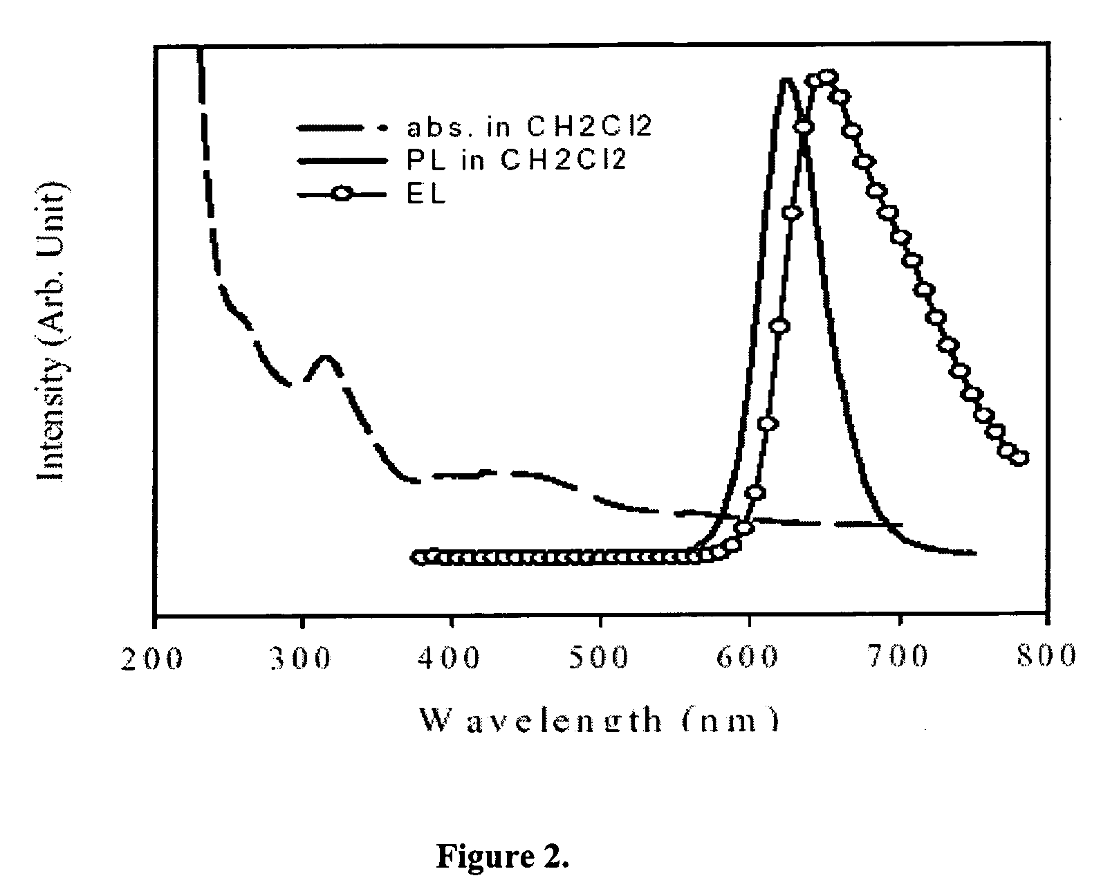
[0078] 1,4-bis(phenyl)phthalazine (FW=282.34, 370 mg, 1.34 mmol) and Ir(acac)3 (FW=489.54, 164.3 mg, 0.336 mmol) were dissolved in degassed glycerol (10 ml). The reaction mixture was refluxed (220° C.) under nitrogen for 10 hours. Purple color precipitates turned out gradually during reflux. After reaction, the crude product was collected by filtration, washed with hexane and ether, dried in a vacuum (yield: 57%). It was then purified by flash-chromatographed on a silica gel column using dichlormethane as eluent. Addition of methanol to the solution followed by heating to boiling to evaporate dichloromethane resulted in precipitation of the product as dark-red color shining particles (40% yield). Melting point: 385.3° C.; 1H NMR: (Chloroform-d, 300 MHz) δ: 8.81 (d, 3H), 8.14 (d, 3H), 7.91 (d, 3H), 7.71 (t, 3H), 7.66 (m, 6H), 7.12 (m, 9H), 6.87 (t, 6H), 6.78 (d, 6H); MS: m / z (%) 1037.0 (100, M+), 755 (15, M+-BPPa); Calc. For C60H39N6Ir (FW=1036.32): ...

example 3

The Procedure of Electroluminescence Device Fabrication

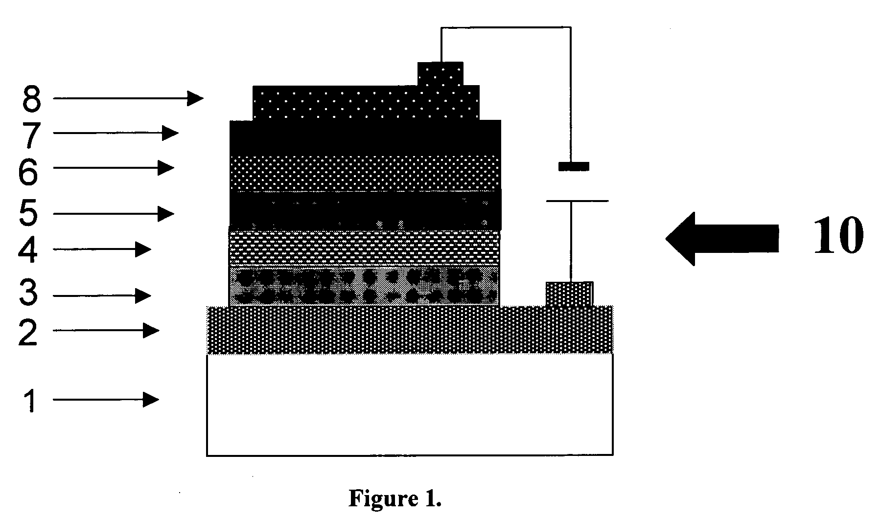
[0079] An indium-tin-dioxide (ITO) coated glass substrate was sequentially untrasonicated in a detergent, rinsed in deionized water and exposed to UV light for 20 minutes, dried. A hole transporting layer of N,N′-bis-(1-naphthyl)-N,N′-diphenylbenzidine was deposited on ITO anode at the vacuum deposition rate about 15 nm / min. by using a tantalum boat to form a thickness of 60 nm. A light-emitting layer of CBP doped with a material with formula [I], [II], [III] was then co-deposited onto the hole-transporting layer with a thickness about 30 nm. The concentration of dopants can be controlled by deposition rate according to the requirement. At the following step, a hole blocking layer of TPBI was deposited onto the light-emitting layer with a thickness about 30 nm. An electron-transporting layer of AlQ3 was deposited onto the light-emitting layer with a thickness about 30 nm Then, a cathode consisted of a 10 / 1 atomic ratio of Mg / Ag...


PUM

PropertyMeasurementUnit
Luminescenceaaaaaaaaaa

Abstract

This invention relates to an organic electroluminescence (EL) device and to the use of a tris-cyclometalated iridium complex with a 3-Phenyl-azine ligand for thin-film type organic electroluminescence devices. The iridium complexes used have the following formulae:

Description

FIELD OF THE INVENTION [0001] This invention relates to an organic electroluminescence (EL) device and to the use of a tris-cyclometalated iridium complex with a 3-Phenyl-azine ligand for thin-film type organic electroluminescence devices. BACKGROUND [0002] Historically, the efficiencies and lifetimes of organic electroluminescence (“EL”) devices were much lower than those obtained from inorganic systems. Therefore, research mainly focused on inorganic materials. [0003] The reason for the low luminance of the early organic EL device is the highly resistive EL medium, which prevents the efficient injection of carriers into the light-emitting layer. Tang and VanSlyke addressed this problem in the late 1980s (Tang and VanSlyke, Appl. Phys. Lett. 1987, 51, 913) by using a structure made of two ultra thin layers: a hole transporting layer of an organic substance laminated on an organic emitting layer. This work revived the research on organic EL devices, and resulted in the development o...

Claims


Application Information

Patent Timeline
IPC IPC(8): C07F15/00H01J1/62
CPCC07F15/0033C09K11/06C09K2211/1044H05B33/14H01L51/0071H01L51/0085H01L51/5016C09K2211/185H10K85/657H10K85/342H10K50/11H10K2101/10
Inventor LEE, SHUIT TONGLEE, CHUN SINGMI, BAOXIUWANG, PENG-FEI
Owner CITY UNIVERSITY OF HONG KONG
Learn More