

Semiconductor device and manufacturing method thereof and method for writing memory element
- Summary
- Abstract
- Description
- Claims
- Application Information
AI Technical Summary
Benefits of technology
Problems solved by technology
Method used
Image

Examples
embodiment mode 1
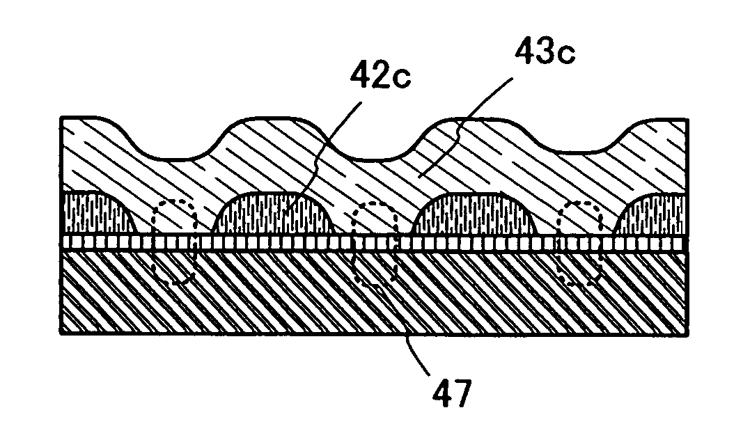
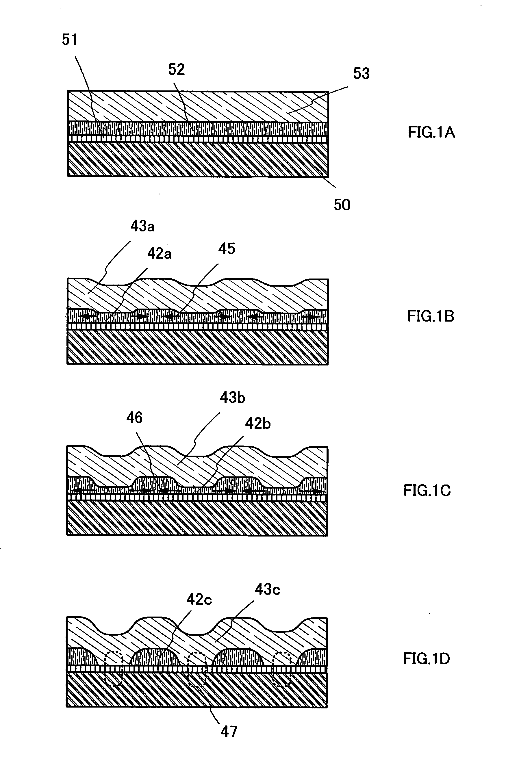
[0042] In this embodiment mode, one example of a structure of a memory element included in a memory device of the invention is described with reference to drawings. More specifically, a structure of a passive matrix memory device is described.
[0043] A memory element of the invention and an operation mechanism thereof are described with reference to FIGS. 1A to 1D and FIGS. 9A to 9C. In this embodiment mode, an insulating layer having low (bad) wettability against an organic compound material used for an organic compound layer is formed between the organic compound layer that constitutes a memory element included in a memory device and at least one of a pair of conductive layers that are formed with the organic compound layer interposed therebetween. By providing the insulating layer, properties of the memory element are not varied and become stable; therefore, normal writing can be carried out.
[0044] The insulating layer is only required to be provided between the conductive layer...
embodiment mode 2
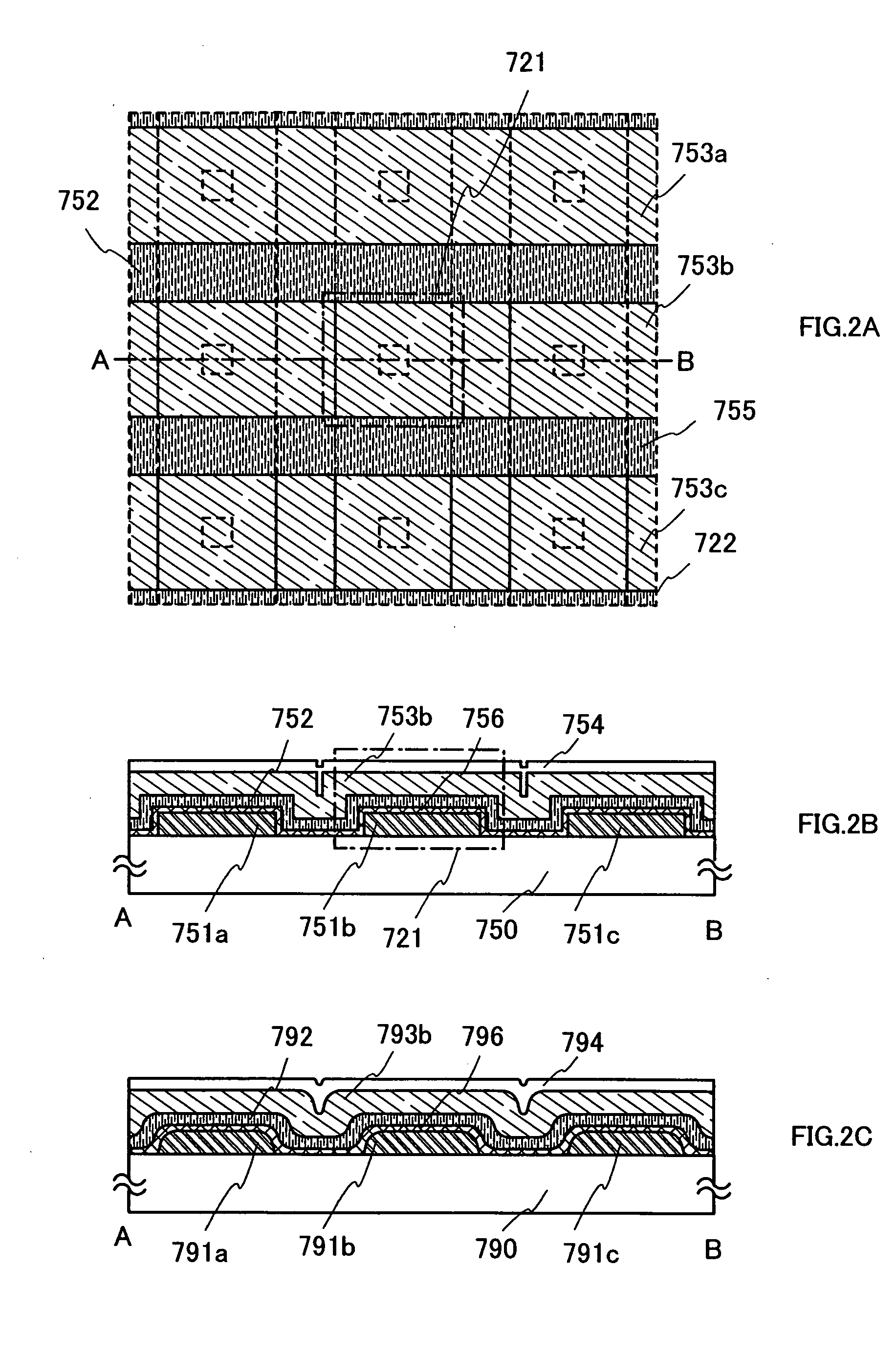
[0101] In this embodiment mode, a memory device having a structure different from that of Embodiment Mode 1 is described. Specifically, a structure of an active matrix memory device is described.
[0102]FIG. 5 shows one configuration example of the memory device that is described in this embodiment mode, which includes a memory cell array 232 in which memory cells 231 are provided in matrix; a bit line driver circuit 226 that has a column decoder 226a, a reading circuit 226b, and a selector 226c; a word line driver circuit 224 that has a row decoder 224a and a level shifter 224b; and an interface 223 that carries out interactions with the outside and has a writing circuit and the like. Note that the configuration of a memory device 217 shown here is only one example, and it may include another circuit such as a sense amplifier, an output circuit, or a buffer, and the writing circuit may be provided in the bit line driver circuit.
[0103] The memory cell 231 has a first wire that const...
embodiment mode 3
[0129] In this embodiment mode, an example of a semiconductor device that has the memory device described in the aforementioned embodiment modes is described with reference to the drawings.
[0130] A semiconductor device described in this embodiment mode is capable of reading and writing data without contact. A data transmission method is broadly classified into an electromagnetic coupling method of communicating by mutual induction with a pair of coils disposed in the opposed position, an electromagnetic induction method of communicating by an inductive electromagnetic field, and a radio wave method of communicating by using radio waves, and any of these methods may be employed. An antenna that is used for transmitting data can be provided in two ways. One way is to provide an antenna over a substrate provided with a plurality of elements and memory elements, and the other way is to provide a terminal portion over a substrate provided with a plurality of elements and memory elements...
PUM
| Property | Measurement | Unit |
|---|---|---|
| Thickness | aaaaa | aaaaa |
| Thickness | aaaaa | aaaaa |
| Electrical conductivity | aaaaa | aaaaa |
Abstract
Description
Claims
Application Information