Light-emitting diode and process for producing the same

a technology of light-emitting diodes and diodes, which is applied in the direction of basic electric elements, electrical apparatus, semiconductor devices, etc., can solve the problems of difficult to divide semiconductor wafers, difficult grinding process, and easy breakage of the substrate itself, so as to improve the external quantum efficiency and luminous extracting efficiency of the light-emitting diodes. , the effect of improving the external quantum efficiency and luminous extracting efficiency

Inactive Publication Date: 2006-12-07
TOYODA GOSEI CO LTD
View PDF6 Cites 64 Cited by
  • Summary
  • Abstract
  • Description
  • Claims
  • Application Information

AI Technical Summary

Benefits of technology

[0066] Effects to be obtained by the present invention are as follows.
[0067] That is, according to the first feature of the present invention, when an objective shaping process is carried out through mechanical or physical treatments such as polishing, dicing, and blasting treatments, the physically damaged layer left on the surface of at least one of the output plane and the reflection plane (hereinafter referred to as a physically processed plane or simply a processed plane) can be removed effectively through etching treatment. As a result, light absorption or diffusion of light toward inside of the device caused by the physically damaged layer formed on the processed plane (: the output plane or the reflection plane) can be restrained effectively. Accordingly, external quantum efficiency and luminous extracting efficiency can be improved when the light-emitting diode (LED) is manufactured.
[0068] According to the second feature of the present invention, because amount of light absorbed by the sidewalls of the light-emitting diode or diffused in the diode increases owing to the method of the first feature of the present invention, external quantum efficiency and luminous extracting efficiency of the light-emitting diode can be improved effectively.
[0069] Also, by carrying out the taper part forming process during the shaping process, not only the taper part but also the physically processed plane including the taper part can be etched at one time. In short, the finishing process for etching the processed plane can be carried out along with etching the taper part.
[0070] According to the third feature of the present invention, at least a portion of the taper part forming process can be carried out by carrying out the process for forming the dividing groove. Alternatively, the process for forming the dividing groove may take place of the whole process for forming the taper part. As a result, the taper part forming process can be carried out quite effectively according to the third feature of the present invention.
[0071] Especially, each feature of the present invention described above may function effectively with respect to a light-emitting diode at least a portion of whose luminous emission is in a frequency range whose luminous spectrum is at least less than 470 nm. According to the fourth and thirteenth aspects of the present invention, however, large amount of light whose luminous spectrum is less than 470 nm in a frequency range of the objective luminous spectrum of the light-emitting diode may not have bad influence, or absorption of light or diffusion of light in the device, owing to the physically damaged layer. As a result, according to the fourth and thirteenth aspects of the present invention, a light-emitting diode with high luminous efficiency, in which possibility of reducing external quantum efficiency owing to the physically damaged layer is effectively excluded, can be provided.

Problems solved by technology

When the substrate is grinded to be too thin, the substrate itself becomes easy to break and the grinding process may take too much time, which is not desirable.
When the substrate is too thick, it becomes difficult to divide the semiconductor wafer into each desired shape precisely and surely, which is not desirable.

Method used


Image

  • Light-emitting diode and process for producing the same
  • Light-emitting diode and process for producing the same
  • Light-emitting diode and process for producing the same

Examples


embodiment 1

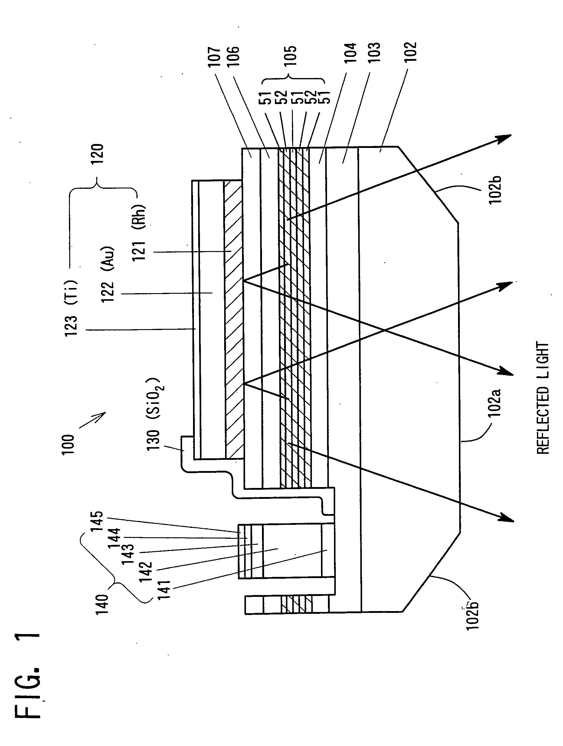
[0101]FIG. 1 is a sectional view of a face-down type light-emitting diode 100 of the present embodiment. The back surface of a semiconductor crystal substrate 102 which has a thickness of about 150 μm and is made of undoped GaN bulk crystal comprises a polished plane 102a which is flattened through dry-etching and a polished plane 102b which is formed in a taper shape and is flattened through dry-etching. As a crystal growth plane which is almost parallel to the polished plane 102a of the semiconductor crystal substrate 102, c plane of the GaN bulk crystal is applied. About 4.0 μm in thickness of silicon (Si) doped gallium nitride (GaN) n-type contact layer 103 is deposited through crystal growth on the crystal growth plane.

[0102] The n-type contact layer 103 has an impurity (Si) concentration of about 1×10¹⁹ / cm3. About 10 nm in thickness of GaN n-type clad layer (low carrier concentration layer) 104 is formed on the n-type contact layer 103.

[0103] On the n-type clad layer 104, ab...

second embodiment

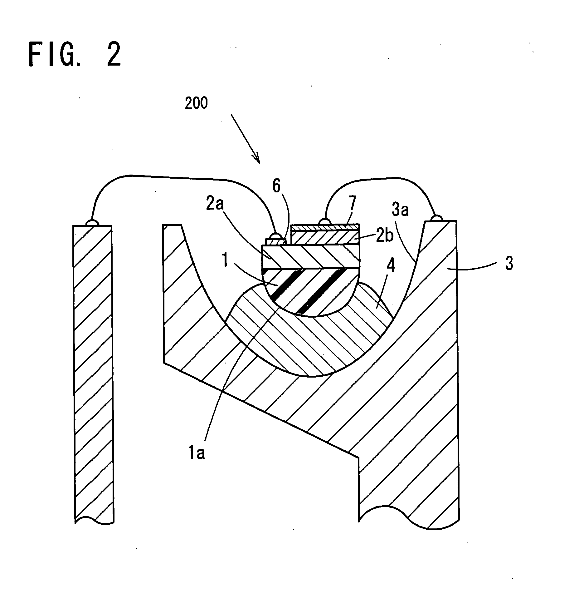
[0164] In a process of forming dividing grooves by applying laser irradiation, a fused and re-solidified material, which is a material of a semiconductor fused by laser irradiation heat, and a fused, scattered and re-solidified material, which is a material fused and scattered in a chamber and then adhered and solidified there, tend to be left at the sidewalls and the back surface of the device. Such fused and re-solidified material and fused, scattered and re-solidified material may preferably be removed through blast treatment and so on considering external quantum efficiency and luminous extracting efficiency. Even by employing such blasting treatment, however, a physically damaged layer as in the first embodiment may be formed owing to some conditions of the treatment. Accordingly, the present invention is also useful for a device in which the physically damaged layer is formed through blasting treatment.

[0165]FIG. 2 is a sectional view of a face-up type light-emitting diode 20...

third embodiment

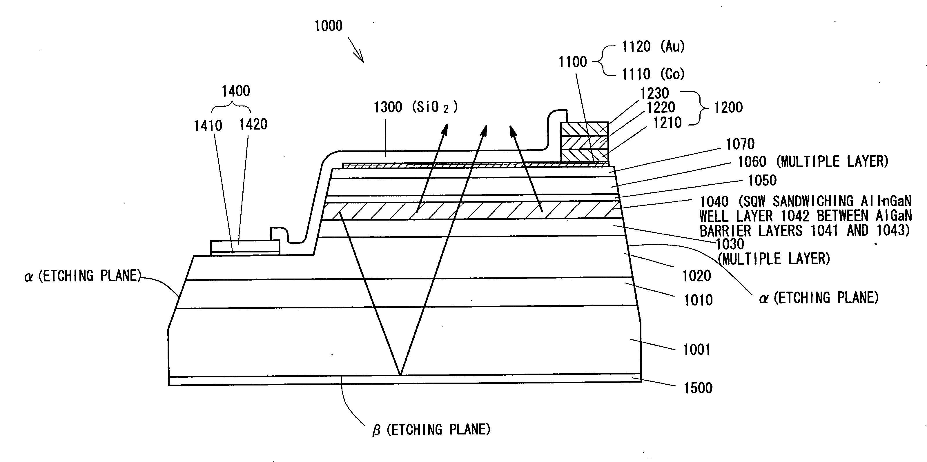
[0169] In the first embodiment, the taper part is formed at the semiconductor crystal substrate 102. Alternatively, the taper part for extracting light may be formed at the sidewall of each semiconductor layer (103-107) deposited through crystal growth to face to the surface of the wafer. The taper part deposited on formed on the side wall near the surface of semiconductor layers functioning as a device also contributes to improve luminous extracting efficiency and external quantum efficiency. A similar taper part tends to be formed at the surface of the wafer when a V-shaped groove for dividing chip is formed on the surface of the wafer. These taper parts can be formed by using, for example, a dicing cutter. And the etching treatment (finishing treatment) is useful for each of thus-obtained taper parts.

[0170] Such characteristics are explained in the third embodiment.

[0171]FIG. 3 is a sectional view of a face-up type light-emitting diode 1000 in the third embodiment of the presen...


PUM


Abstract

The back surface of a semiconductor crystal substrate 102 which has a thickness of about 150 μm and is made of undoped GaN bulk crystal consists of a polished plane 102a which is flattened through dry-etching and a grinded plane 102b which is formed in a taper shape and is flattened through dry-etching. On about 10 nm in thickness of GaN n-type clad layer (low carrier concentration layer) 104, about 2 nm in thickness of Al0.005In0.045Ga0.95N well layer 51 and about 18 nm in thickness of Al0.12Ga0.88N barrier layer 52 are deposited alternately as an active layer 105 which emits ultraviolet light and has MQW structure comprising 5 layers in total. Before forming a negative electrode (n-electrode c) on the polished plane of the semiconductor substrate a, the polished plane is dry-etched.

Description

TECHNICAL FIELD [0001] The present invention relates to structure of a light-emitting diode and a method for fabricating the same. More particularly, the present invention deeply relates to external quantum efficiency and luminous extracting efficiency. [0002] Accordingly, the present invention is useful for a LED (light-emitting diode) which has shorter luminous wavelength and emits blue-violet, violet, or ultraviolet light and for a method for fabricating the same. [0003] Also, the present invention relates to a method for forming an electrode on a grinded plane of a semiconductor substrate comprising a conductive Group III nitride compound semiconductor which has already been polished. [0004] The present invention can be widely applied to a semiconductor device in which an electrode is formed directly on its semiconductor substrate. The semiconductor device having such structure may comprise a light-emitting semiconductor device such as a semiconductor laser (LD), a light-emittin...

Claims


Application Information

Patent Timeline
Patent Type & Authority Applications(United States)
IPC IPC(8): H01L21/00H01L33/00H01L33/20H01L33/32
CPCH01L33/32H01L33/20H01L2224/32257H01L24/32H01L2224/32245H01L2224/48091H01L2224/48247H01L2224/48257H01L2224/48464H01L2224/73265H01L2924/10158H01L2924/00014H01L2924/00H01L2924/00012
Inventor ASAI, MAKOTOYAMAZAKI, SHIROKOZAWA, TAKAHIRONARUKAWA, MITSUHISA
Owner TOYODA GOSEI CO LTD
Why Eureka
Try Eureka