Method for fabrication of physical patterns and the method for fabrication of device using the same

a technology of physical pattern and fabrication method, which is applied in the direction of optical recording/reproducing/erasing method, photomechanical apparatus, instruments, etc., can solve the problems of poor reproducibility of process, high processing cost, and high processing cost, so as to reduce increase and achieve the effect of improving the solubility of the region

Inactive Publication Date: 2006-12-07
HITACHI LTD
View PDF13 Cites 6 Cited by
  • Summary
  • Abstract
  • Description
  • Claims
  • Application Information

AI Technical Summary

Benefits of technology

[0012] When a physical pattern is formed by selectively etching the crystalline regions or the amorphous regions of the phase change film, the etching properties can be effectively improved if the surface is treated before such etching so that the regions to be removed by the dissolution and the regions to be left undissolved will have surface conditions different from one another. More specifically, when the regions to be removed by the dissolution are treated to increase the solubility of the region, and the regions to be left undissolved are treated to reduce the solubility of the region, the etching will be facilitated to leave a smooth surface in both the etched and unetched regions. The advance treatment of the present invention is a treatment capable of accomplishing such an effect, an it contributes for the stability of the process by reducing the etching time and by increasing the etching...

Problems solved by technology

In the resist processing using an optical energy, reaction of the resist is proportional to the total amount of the beam such as laser beam that has been irradiated, and limitation is set on the preciseness of the processing.
Production of a high density pattern in this manner, however, requires use of an extremely low power.
This invites poor reproducibility of the process as well as significant decrease in the yield of the pattern and the device.
The processing using thermal energy as described in Japanese Journal of Applied Physi...

Method used


Image

  • Method for fabrication of physical patterns and the method for fabrication of device using the same
  • Method for fabrication of physical patterns and the method for fabrication of device using the same
  • Method for fabrication of physical patterns and the method for fabrication of device using the same

Examples


first embodiment

[0032] A ROM substrate for an optical disk was produced by using a phase change film which is used in most optical disks by the method as described above.

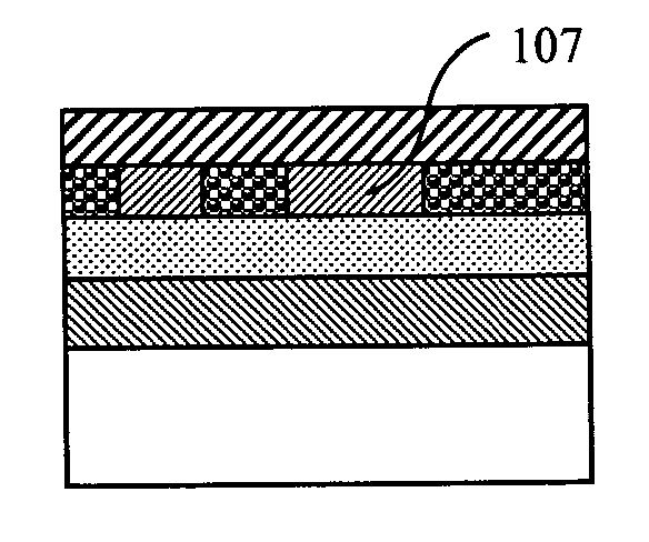
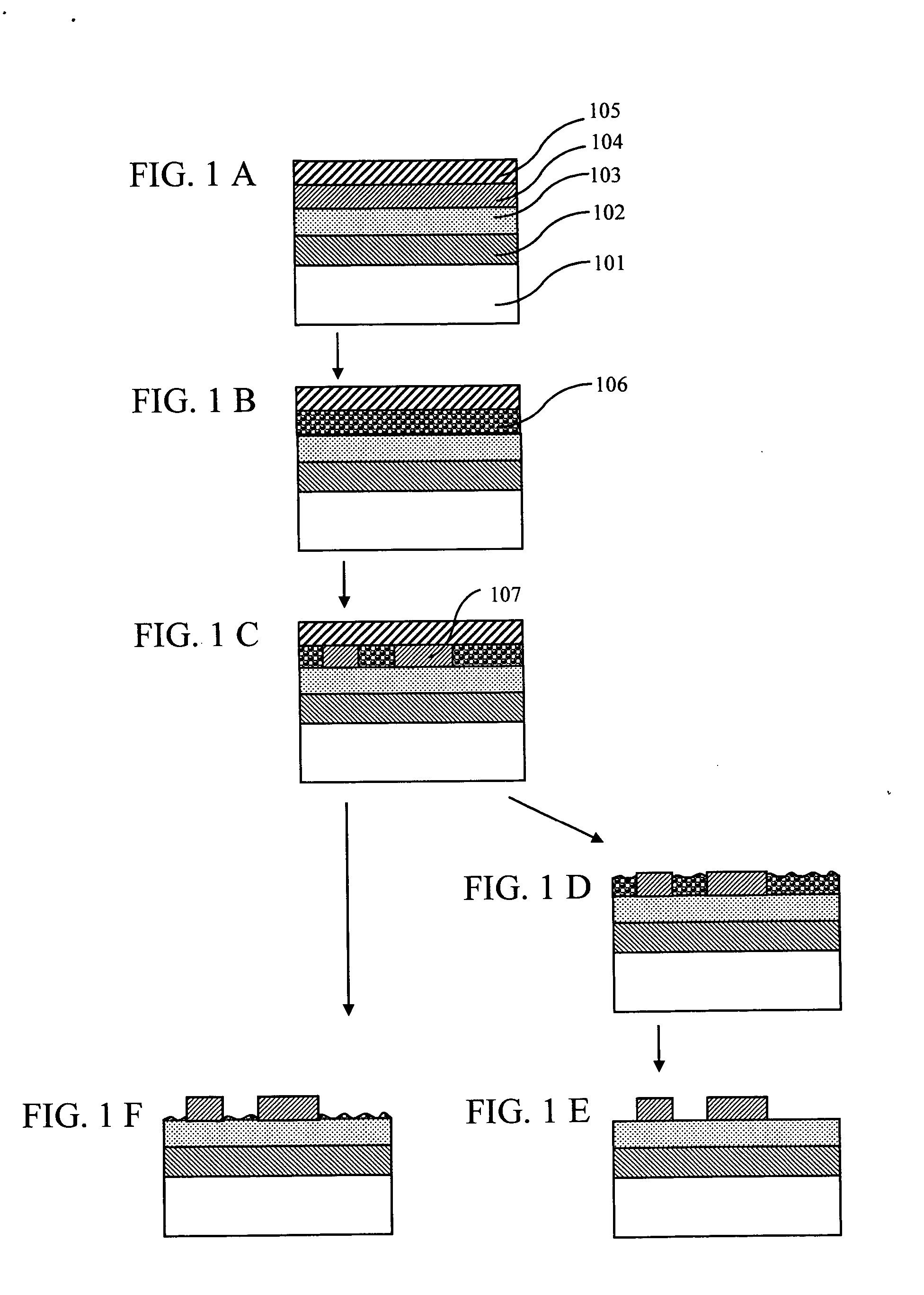
[0033] A medium having the structure of FIG. 1A was produced, and, an attempt was made to record amorphous marks by irradiating the medium with a laser beam. The medium comprises a glass substrate 101, and an Ag film 102, a lower protective film 103, a phase change film 104, and a protective film 105 disposed on the substrate 101 in this order. All of the film layers formed on the glass substrate 101 were formed by sputtering. The protective film 105 was formed from SiO2, and the lower protective film 103 was formed from (ZnS)80(SiO2)20, and the phase change film 104 was formed form Ge5Sb70Te25. The Ag film 102 was formed to diffuse the heat generated within the phase change film by the laser irradiation.

[0034] This medium was heated in a bake furnace to a temperature of 300° C. for 3 minutes to crystallize the phase change film ...

second embodiment

[0038] Another method for producing a physical pattern is shown in FIG. 4. In this method, a plastic substrate was used and the recording was accomplished by using a commercially available recording system. A polycarbonate substrate was used for the plastic substrate. As shown in FIG. 4A, a disk comprising a lower protective film 402, a phase change film 403, a upper protective film 404, a reflective film 405, and a polycarbonate upper substrate 406 disposed on a lower substrate 401 was produced. The films were all formed by sputtering, and the reflective film 405, the upper protective film 404, the phase change film 403, and the lower protective film 402 were deposited on the upper substrate 406 in this order. The reflective film 405 was an Ag film having a thickness of 20 nm, and the upper protective film 404 was a film of ZnS—SiO2 having a thickness of 30 nm. The phase change film 403 was a film of Ge5Sb70Te25 having a thickness of 20 nm, and the lower protective film 402 was a f...

third embodiment

[0043] In this embodiment, the advance treatment was accomplished by reactive ion etching. The surface of the region having a thermal energy applied thereto and the surface having no such thermal energy applied, or the regions having the thermal energy applied under different conditions experienced different reactions when such surfaces were further treated by slow reactive ion etching at a low power.

[0044] A disk was produced by repeating the procedure of the second embodiment, and after exposing the phase change film on the surface, the surface was treated-by reactive ion etching (RIE). The RIE was conducted for 20 seconds at a power of 100 W by using CHF3 for the gas.

[0045] In order to evaluate the difference in the fluoride formation on the surface, a sample having a line-shaped amorphous region formed in the crystalline region was prepared and this sample was immersed in water. When it was removed from the water, the water was immediately shed by the crystalline region while ...


PUM


Abstract

Etching properties are improved in a processing method of a phase change material in which the regions of one state are removed by etching to form a fine physical pattern. The phase change film is subjected to an advance treatment conducted before the etching, and this advance treatment uses water, an alkaline solution, an acid solution, or a surface-active agent. The regions to be removed by the etching are treated in the advance treatment to facilitate penetration of the etchant in the etching step so that complete removal is accomplished with no film residue. The advance treatment also improves etching resistance of the regions to be left unremoved. The process is thereby stabilized.

Description

[0001] CROSS REFERENCE TO RELATED APPLICATION [0002] U.S. Patent application No. 11 / 051,143 is a co-pending application of this application. The content of which is incorporated herein by cross-reference.CLAIM OF PRIORITY [0003] The present application claims priority from Japanese Applications JP 2005-162513 filed on Jun. 2, 2005, the content of which is hereby incorporated by reference into this application. FIELD OF THE INVENTION [0004] This invention relates to a method for forming a fine physical pattern. BACKGROUND OF THE INVENTION [0005] Methods for imparting a material with a physical pattern by using the difference in physical or chemical properties between the region having an energy applied and the region having no such energy applied can be divided into two categories: those wherein the energy used is an optical energy and those wherein the energy used a thermal energy. In the field of semiconductors and optical disks, methods using an optical energy is generally known, ...

Claims


Application Information

Patent Timeline
IPC IPC(8): G03C5/00
CPCG11B7/00454G11B7/266
Inventor ANZAI, YUMIKOSHINTANI, TOSHIMICHI
Owner HITACHI LTD
Why Eureka
Try Eureka