Information read device and read signal processing circuit

a signal processing circuit and information read technology, applied in the direction of digital signal error detection/correction, amplitude demodulation, pulse technique, etc., can solve the problems of phase detector used in a pll being affected by noise in the input signal, increasing error rate, and increasing frequency fluctuation in the read clock. , to achieve the effect of suppressing noise, improving snr (signal-to-noise ratio), and increasing error ra

Active Publication Date: 2006-12-14
HITACHI CONSUMER ELECTRONICS CORP
View PDF7 Cites 60 Cited by
  • Summary
  • Abstract
  • Description
  • Claims
  • Application Information

AI Technical Summary

Benefits of technology

[0006] The read clock must synchronize with the read signal clock with adequate accuracy in order to obtain a satisfactory effect from the Viterbi decoder in the PRML signal processing system. However, the phase detector used in a PLL is affected by noise in the input signal. So the problem then occurs that when the input signal SNR (signal-to-noise ratio) of the PLL phase detector drops, the frequency fluctuation in the read clock becomes larger, so that the error rate increases. When the input signal contains components with drastically low resolution, the effects of fluctuations in noise and (DC) direct current components are compounded and cause the problems of poor phase error detection accuracy or mistakenly detecting the pulse edge.
[0007] In order to resolve the above problems, the present invention contains a selector for selecting an output from the adaptive type equalizer (FIR EQ, Adaptive EQ) for equalizing the AD converted digital signals, and an output from a short FIR equalizer (for example, a limit equalizer) for equalizing the AD converted digital signal and; inputting that output to the phase detector in the PLL circuit. Under normal operating conditions, the low-pass filter characteristics of the FIR equalizer act to suppress noise in the high-frequency region and therefore improve the SNR (signal-to-noise ratio) of the signal input to the phase detector. However, the loop delay of the PLL circuit then increases. The short FIR equalizer on the other hand renders no noise suppression effect, yet if the short FIR equalizer contains a limit equalizer, then it can greatly amplify only the 2T length signal even if there are only a small number of taps, so the short FIR equalizer can improve the jitter in the signal input to the phase detector.
[0008] This optical disk signal processing system achieves a low error rate even when the SNR (signal-to-noise ratio) of the input signal is low, and avoids pulse edges with low phase detection accuracy or signal pulse strings with a high possibility of being mistakenly detected as an edge in conventional methods, and also supports diverse types of input signals.

Problems solved by technology

However, the phase detector used in a PLL is affected by noise in the input signal.
So the problem then occurs that when the input signal SNR (signal-to-noise ratio) of the PLL phase detector drops, the frequency fluctuation in the read clock becomes larger, so that the error rate increases.
When the input signal contains components with drastically low resolution, the effects of fluctuations in noise and (DC) direct current components are compounded and cause the problems of poor phase error detection accuracy or mistakenly detecting the pulse edge.
However, the loop delay of the PLL circuit then increases.

Method used


Image

  • Information read device and read signal processing circuit
  • Information read device and read signal processing circuit
  • Information read device and read signal processing circuit

Examples


first embodiment

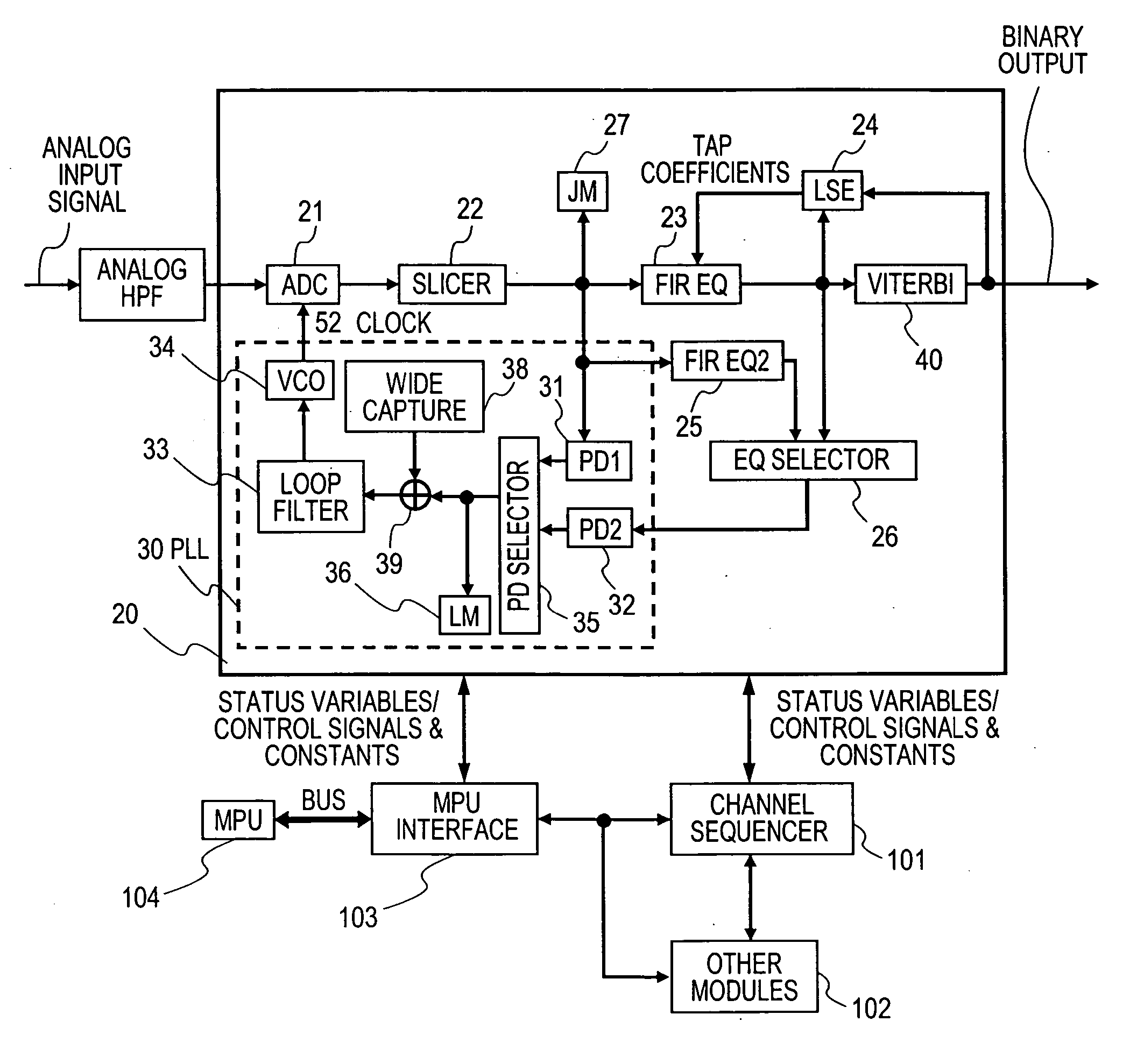
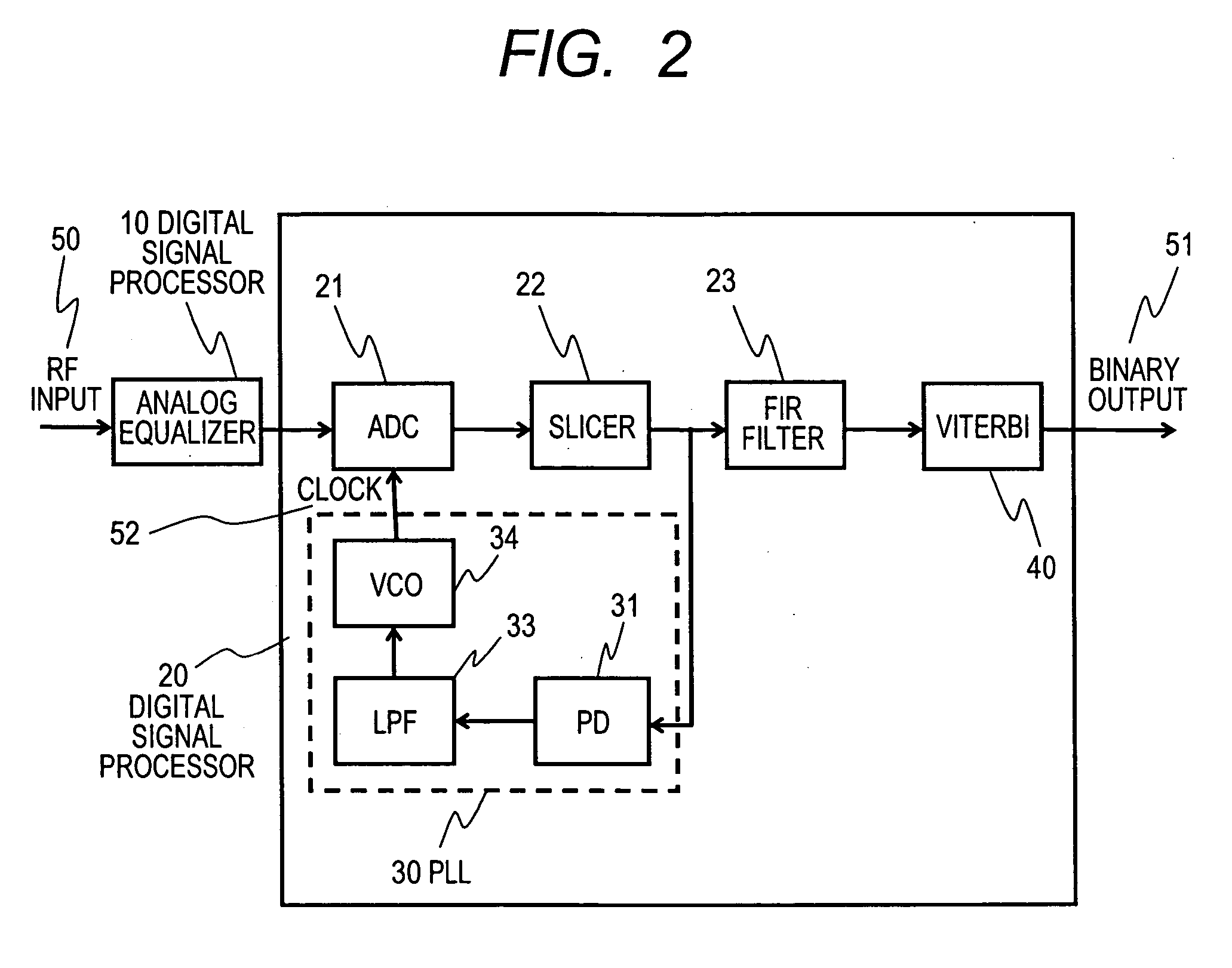
[0037]FIG. 1 is a drawing showing the structure of the decoder circuit for the read signals of the present invention. After AGC and equalization processing by the analog equalizer, the RF signal detected by the optical head not shown in the drawing is input to a digital signal processor 20. After the input RF signals are changed to digital signal per each clock by the AD converter 21, these signals are DC compensated in a slicer 22, digitally processed in the FIR equalizer 23, binarized by a Viterbi decoder 40, and extracted as a binarized output 51. The Viterbi decoder 40 compares the read signal with the target signal generated from the convolution of the PR class and the bit stream, and selects and binarizes a bit stream with a minimal error (difference). The LSE (least square error) controller 24 implements processing for adapting to the tap coefficient of the FIR equalizer described above. The PLL (Phase Locked Loop) circuit 30 that generates a clock signal 52 includes a two ph...

second embodiment

[0042] Various sequences (procedures) are defined in the channel sequencer. These sequences are executed when there is a request from the MPU based on firmware instructions or by taking advantage of different types of interrupt requests issued by a mechanism monitoring state variables of different types held internally in the channel sequencer. These sequences are defined in the following embodiments. A priority level is assigned to each interrupt, and for example, when an interrupt with a high level of priority has been issued during processing for a low priority interrupt, then the on-going processing is halted and the processing for the high priority interrupt is performed first. The priority level for the interrupt can be changed as needed.

[0043] During phase detection utilizing the output of the FIR equalizer or the short FIR equalizer 25, the procedure shown in FIG. 5 is for a mode utilized exclusively when the quality of the read signal that was input is within the range spe...

third embodiment

(Maintaining the PLL Lock)

[0047] A sequence for monitoring the state after completion of PLL pull-in and maintaining the lock is shown in FIG. 6. This sequence is executed if the PLL is unlocked so the channel sequencer must monitor the output of the lock monitor. The process for monitoring the lock monitor output is actually performed by the channel sequencer as previously described, and the expressions contained in this sequence are shown in FIG. 6. These type of expressions are for the purpose of clarifying that the observation variables for the sequence are the lock monitor. These same expressions are used even in flowcharts in other embodiments from hereon for describing the sequence.

[0048] When the PLL pull-in sequence is complete (PLL is in locked state), the PLL shifts to a mode to maintain the lock state. In other words, the sequence shown in FIG. 6 for the pull-in mode that was disabled in pull-in mode is now enabled. As shown in FIG. 6, the lock monitor output is monit...


PUM

PropertyMeasurementUnit
phase erroraaaaaaaaaa
sizeaaaaaaaaaa
lengthsaaaaaaaaaa

Abstract

An optical disk read signal processing system for Blu-ray disc systems to ensure stable phase-locked locked operation even with a low signal-to-noise ratio. This system changes a loop configuration of a phase lock loop circuit according to the operating state, and utilizes a FIR equalizer for phase detection. This system attains a low error rate even when the signal-to-noise ratio of an input signal is low, and avoids pulse edges with low phase detection accuracy or signal pulse streams with a high possibility of being mistakenly detected as an edge in conventional methods, and also supports diverse types of input signals.

Description

CLAIM OF PRIORITY [0001] The present application claims priority from Japanese application JP 2005-168979 filed on Jun. 9, 2005, the content of which is hereby incorporated by reference into this application. FIELD OF THE INVENTION [0002] The present invention relates to an information read device for reading information written on a recording medium, as well as a read signal processing circuit for processing read signals. BACKGROUND OF THE INVENTION [0003] In recent years, the PRML (partial response most-likelihood) method is utilized in systems for processing read signals in optical disk drives such as for DVD (digital versatile disc). This read method is already widely used in the communications field and information recording devices such as magnetic tape units and hard disk drives and so is a convenient method for achieving low bit error rates even under conditions where there is strong inter-symbol interference. Therefore this PRML method is particularly effective for boosting...

Claims


Application Information

Patent Timeline
Patent Type & Authority Applications(United States)
IPC IPC(8): H03H7/30H03D1/00H03D3/24G11B7/005G11B20/14G11B20/18
CPCG11B20/10009G11B20/10046H04L7/0004G11B20/10425G11B20/10222
Inventor KIKUGAWA, ATSUSHIMINEMURA, HIROYUKI
Owner HITACHI CONSUMER ELECTRONICS CORP
Why Eureka
Try Eureka