Downconverter and upconverter

a technology of upconverter and downconverter, which is applied in the direction of demodulation, electrical apparatus, transmission noise suppression, etc., can solve the problems of inability to meet the associated requirement specification, low-if scheme cannot be applied, and circuit size significantly increases, so as to reduce power consumption, improve the error vector magnitude (evm), and reduce the effect of power consumption

Inactive Publication Date: 2006-12-14
SAMSUNG ELECTRONICS CO LTD
View PDF19 Cites 65 Cited by
  • Summary
  • Abstract
  • Description
  • Claims
  • Application Information

AI Technical Summary

Benefits of technology

[0053] Accordingly, the present invention has been designed to solve the above and other problems. Therefore, it is an object of the present invention to provide a downconverter and upconverter that can reduce power consumption, obtain a sufficient image rejection ratio in a low-Intermediate Frequency (IF) scheme, and improve Error Vector Magnitude (EVM) in a zero-IF scheme.

Problems solved by technology

In this case, there is a problem in that circuit size significantly increases.
However, there is a problem in that an associated requirement specification cannot be satisfied and the low-IF scheme cannot be applied, when the robustness to interference of more than 30 dB is required.
To achieve precision improvement, a large chip area may be required and costs may increase.
The image rejection ratio of about 30 dB is not a value capable of being easily realized.
In this case, there is a problem in that all characteristics except the image rejection ratio are degraded due to an increase in consumption power and a decrease in a transition frequency, fT.
When the same requirement specification exceeds the image rejection ratio capable of being realized by the image rejection mixer also in the W-CDMA, the channel selection of the digital part is actually impossible.
Accordingly, the low-IF scheme cannot be applied to the digital tuner or the software radio front-end.
However, when the IF signal frequency is increased, existing radio device for performing frequency processing through digital processing have a problem in that power consumption increases due to a clock increase in an analog-to-digital converter (ADC) for converting an IF signal to a digital signal and a digital signal processor for processing an output of the ADC.
In this case, an input frequency band of the ADC is widened, such that power consumption increases as before the clock reduction in the ADC.
There is a problem in that power consumption increases if the IF signal frequency also increases when the IF signal is processed in an analog form.
However, there is a problem in that power consumption increases according to a computational process in a digital using a digital correction process.
There is another problem in that a size of a correction circuit for a correction based on an analog process increases and correction precision is poor.
This method has a problem in that loss occurs in the phase shifter.
Due to this loss, reception sensitivity is degraded.
The method has another problem in that practical precision cannot be obtained in the phase shifter configured as a Resistor-Capacitor (RC) circuit when input / output impedance is considered because R and C values are small in the RF of a high frequency.
However, there are problems in that power consumption increases because the number of mixers and the number of local signal oscillators are increased to generate complex signals from the mixers using complex local signals and spurious reception occurs due to the increased number of local signal oscillators.
When a variable RF filter for obtaining an attenuation amount required for the image frequency is not used, an image rejection ratio cannot be ensured.
Therefore, a filter size increases and fine adjustment is required for pass band characteristics of the filter, because an allowable error is small when variation or tuning is made in relation to cutoff characteristics.
When the frequency of the second IF signal is low, the first IF filter is required to have very steep transition band characteristics and has a problem in that a filter size or filter insertion loss increases.
In this case, there is a problem in that a requirement specification for the first IF filter is strict.
There is a problem in that power consumption increases due to an increase in a clock frequency of the ADC or an increase in an input bandwidth of the ADC adopting the sub-nyquist sampling.
However, the structure based on the low-IF scheme has a problem in that the image rejection ratio of about 30 dB is only ensured as in the single-conversion downconverter.
A method for improving the image rejection ratio is followed by an increase in power consumption like the improvement method for the single-conversion downconverter.
Therefore, there is a problem in that cost and power consumption increase in an IF signal processor.
Moreover, there is a problem in that a strict requirement specification is applied for the RF filter when the IF signal frequency is desired to be reduced.
In some cases, a SAW filter for the RF signal is unnecessary.
This exceeds an allowable mask of the spurious transmission component and does not satisfy the specification.
There is a problem in that an associated specification may not be stably satisfied because the image rejection ratio may be reduced due to variation of the image rejection mixer or variation of environment conditions, even though the specification of an associated spurious mask can be almost satisfied.
However, the frequency of the IF signal cannot be reduced to mitigate the requirement of the RF filter.
As described above, there is a problem in that the cost and power consumption of the IF signal processor increase.
Because of the inaccuracy of an analog circuit, it is difficult for an image rejection ratio for satisfying the specification to be obtained.
However, because the method is theoretically excellent but the polyphase filter is implemented with an RC circuit, loss becomes large and a band becomes narrow.
There are problems in that loss is further increased, the image rejection ratio of a filter output is reduced, and utility is degraded when the number of steps increases to obtain a high attenuation level or a wide band.
However, this method has a problem of an increase of consumption power and a problem of spurious reception occurs due to the increased number of local signal oscillators because the number of mixers and the number of local signal oscillators are increased.
A problem of a DC offset occurs when leakage of the local signal is self-received in the mixer.
When the second-order intermodulation (IM2) occurs due to non-linearity of the mixer, a problem of interference to a target signal occurs due to distortion.
In this case, a problem of the Error Vector Magnitude (EVM)-related degradation occurs.
When multi-level modulation is performed at a high communication rate, EVM-related degradation becomes an important problem.
When real and imaginary part signals I and Q of a local signal are not completely orthogonal after processing in the mixer, the problem of the EVM-related degradation due to incompleteness occurs as described above.
However, the improvement of circuit characteristics is limited because of incompleteness of an analog circuit.
Specifically, degradation due to interference between codes in the multi-level modulation and degradation due to interference between carriers in Orthogonal Frequency Division Multiplexing (OFDM) occur.
There is a problem in that a practical communication rate is less than a theoretical upper limit and high-speed communication is interrupted because of a limit of error improvement.
Moreover, compensation technology in a digital signal process has a problem in that an increase in throughput is followed by an increase in power consumption.
That is, there is a problem in that carrier leakage associated with the DC offset in the downconverter of the zero-IF scheme occurs.
Like the downconverter of the zero-IF scheme, the upconverter of the zero-IF scheme has a problem in that the EVM-related degradation due to incompleteness occurs when real and imaginary part signals I and Q of a local signal are not completely orthogonal after processing in the mixer.
Like the downconverter of the zero-IF scheme, the upconverter of the zero-IF scheme has a problem in EVM improvement.
The important problems in the downconverter and upconverter of the low-IF scheme occur when a sufficient image rejection ratio cannot be obtained and power consumption increases.
The important problems in the downconverter and upconverter of the zero-IF scheme are EVM-related degradation at a high communication rate and an increase in power consumption.

Method used


Image

  • Downconverter and upconverter
  • Downconverter and upconverter
  • Downconverter and upconverter

Examples


first embodiment

[0418] V. First Embodiment of Downconverter of Low-IF Scheme

[0419] Next, a first embodiment of a downconverter of a low-IF scheme in accordance with the present invention will be described with reference to the accompanying drawings.

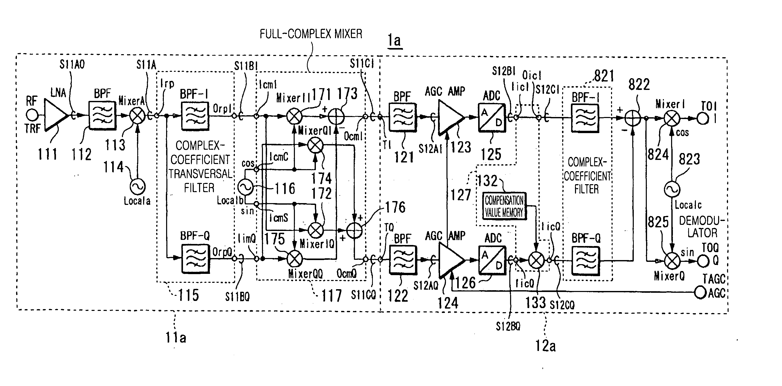
[0420]FIG. 25 is a block diagram illustrating a structure of a downconverter 4 of the low-IF scheme in accordance with an embodiment of the present invention. The downconverter 4 is similar to that of FIG. 19. However, the structures and operations of an IF generator 41 and a baseband generator 42 are different from those of the IF generator 31 and the baseband generator 32 in the downconverter 3 corresponding to the example of the third basic structure.

[0421] Next, the downconverter 4 in accordance with this embodiment will be described with reference to the accompanying drawings.

[0422] The IF generator 41 is different from the IF generator 31 corresponding to the example of the third basic structure, in that the IF generator 41 uses a complex-coeffi...

second embodiment

[0435] W. Second Embodiment of Downconverter Based on Low-IF Scheme

[0436] Next, a second embodiment of the downconverter based on the low-IF scheme in accordance with the present invention will be described with reference to the accompanying drawings.

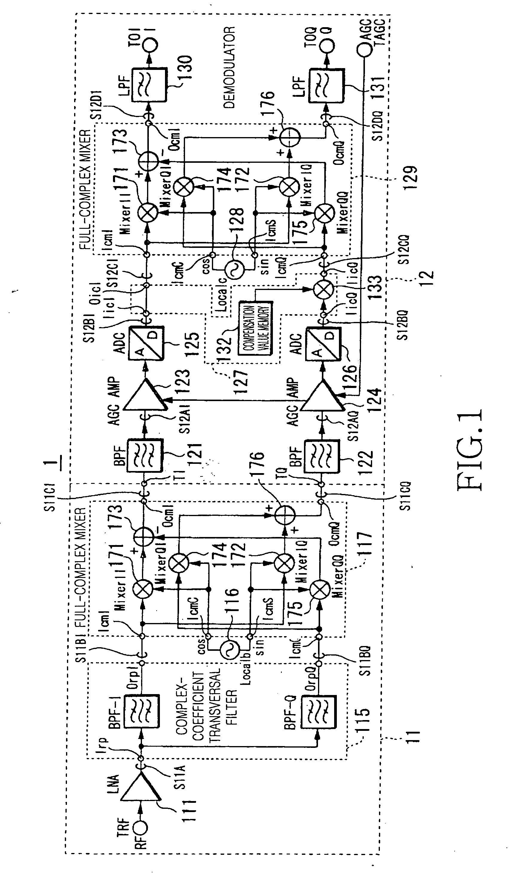
[0437]FIG. 26 is a block diagram illustrating a structure of a downconverter 5 based on the low-IF scheme in accordance with an embodiment of the present invention. The downconverter 5 is similar to that of FIG. 25. However, the structure and operation of a baseband generator 52 are different from those of the baseband generator 42 of the downconverter 4 based on the first embodiment of the present invention. Next, the downconverter 5 in accordance with this embodiment will be described with reference to the accompanying drawings.

[0438] The baseband generator 52 is different from the baseband generator 42 of the first embodiment in that the switch 140 is deleted and an AGC amplifier 124, an ADC 126, a mixer-I 141, a mixer-Q 142, and L...

third embodiment

[0445] X. Third Embodiment of Downconverter Based on Low-IF Scheme

[0446] Next, a third embodiment of the downconverter based on the low-IF scheme will be described with reference to the accompanying drawings.

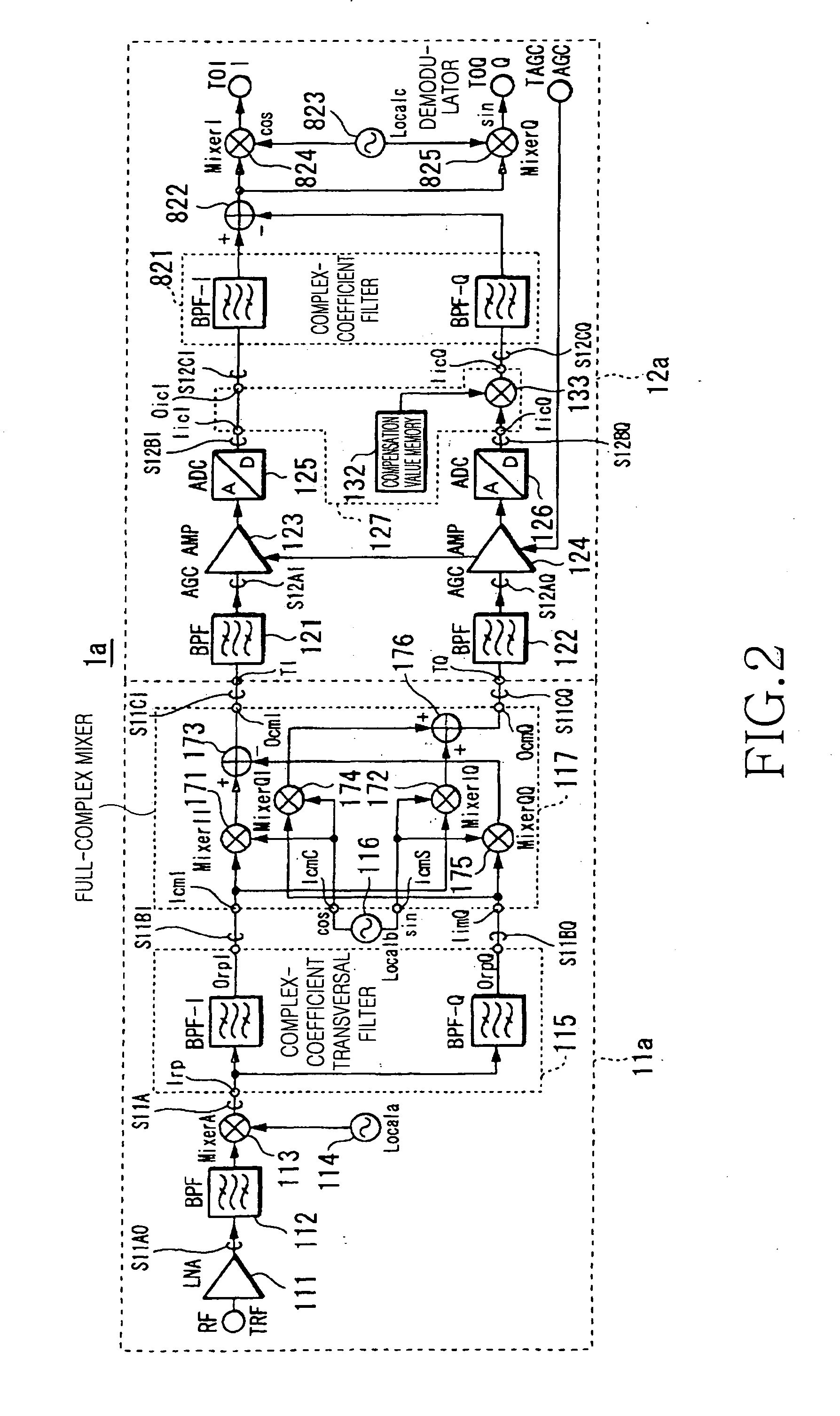
[0447]FIG. 27 is a block diagram illustrating a structure of a downconverter 6 based on the low-IF scheme in this embodiment. The downconverter 6 is similar to that of FIG. 25. However, the structure and operation of a baseband generator 62 are different from those of the baseband generator 42 of the downconverter 4 based on the first embodiment of the present invention.

[0448] Next, the downconverter 6 in accordance with this embodiment will be described with reference to the accompanying drawings. The baseband generator 62 is different from the baseband generator 42 of the first embodiment in that the complex-coefficient SAW filter 340 is replaced with a complex-coefficient SAW filter 350 and the adder 139 and the switch 140 are deleted.

[0449] An output terminal of the compl...


PUM


Abstract

A downconverter and upconverter are provided which can obtain a satisfactory image rejection ratio in a low-Intermediate Frequency (IF) scheme while reducing power consumption, and can improve Error Vector Magnitude (EVM) in a zero-IF scheme. A complex-coefficient transversal filter rejects one side of a positive or negative frequency, and converts a Radio Frequency (RF) signal to a complex RF signal configured by real and imaginary parts. A local oscillator outputs a complex local signal in which a set frequency is set as a center frequency. A full-complex mixer, connected to the complex-coefficient transversal filter and the local oscillator, perform a frequency conversion process by multiplying a complex signal output from the complex-coefficient transversal filter and the complex local signal output from the local oscillator, and outputs a complex signal of a frequency separated by the set frequency from a frequency of the RF signal.

Description

PRIORITY [0001] This application claims priority under 35 U.S.C. § 119 to an application entitled “Downconverter and Upconverter” filed in the Japan Patent Office on Apr. 28, 2005 and assigned Serial No. 2005-133240, the contents of which are incorporated herein by reference. BACKGROUND OF THE INVENTION [0002] 1. Field of the Invention [0003] The present invention relates to a downconverter for performing frequency conversion in a receiver and an upconverter for performing frequency conversion in a transmitter. [0004] 2. Description of the Related Art [0005] a. Background Technology of Downconverter of Low-Intermediate Frequency (IF) Scheme [0006] A communication device which functions both as a receiver and a transmitter like a mobile phone receives a modulated Radio Frequency (RF) signal carrying speech content and data communication content and converts the received RF signal to a frequency to be input to a demodulator. Front-end structures for selecting a channel to select a tar...

Claims


Application Information

Patent Timeline
Patent Type & Authority Applications(United States)
IPC IPC(8): H04B1/26
CPCH04B1/30H03D7/166H04B1/26H03D7/00
Inventor KISHI, TAKAHIKOSATO, TAKAHIRO
Owner SAMSUNG ELECTRONICS CO LTD
Why Eureka
Try Eureka