EL display device
a technology of el and display device, which is applied in the manufacture of electrode systems, cold cathodes, electric discharge tubes/lamps, etc., can solve the problems of devices in the light intensity of el devices, and achieve the effects of reducing the average film resistance of the anode, preventing light leakage, and low electrical resistivity
- Summary
- Abstract
- Description
- Claims
- Application Information
AI Technical Summary
Benefits of technology
Problems solved by technology
Method used
Image

Examples
embodiment 1
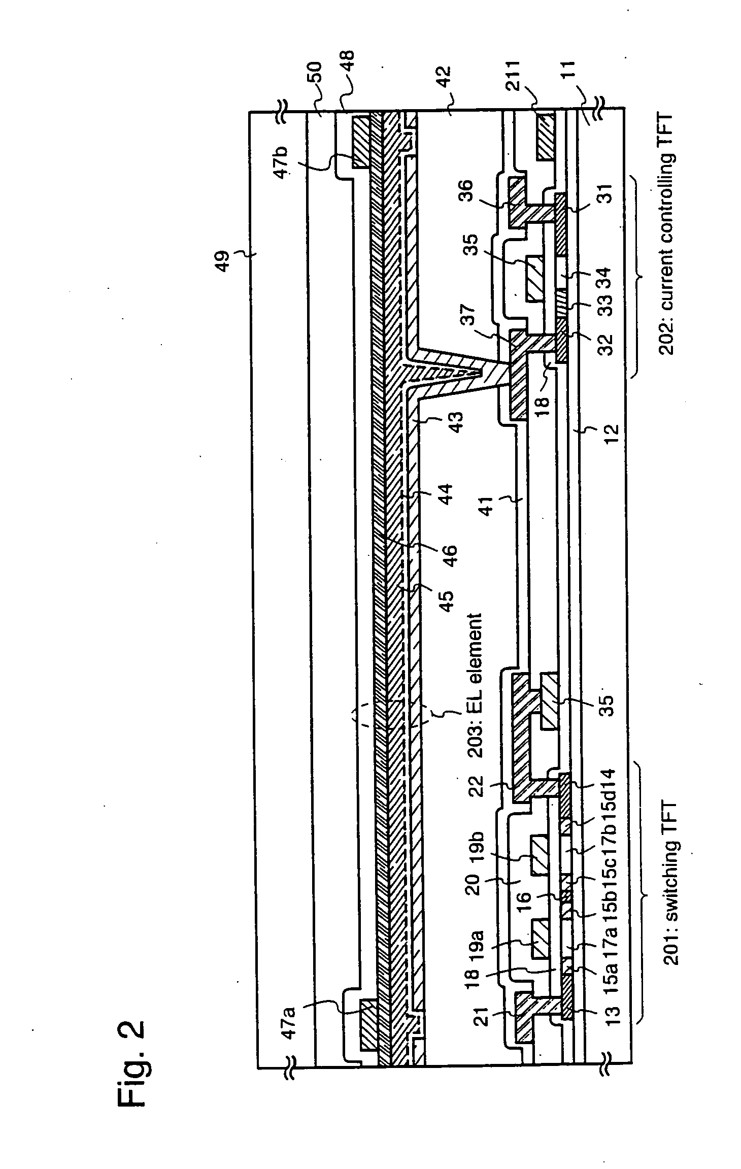
[0091] The embodiments of the present invention are explained using FIGS. 4A to 6C. A method of simultaneous manufacturing of a pixel portion, and TFTs of a driver circuit portion formed in the periphery of the pixel portion, is explained here. Note that in order to simplify the explanation, a CMOS circuit is shown as a basic circuit for the driver circuits.
[0092] First, as shown in FIG. 4A, a base film 301 is formed with a 300 nm thickness on a glass substrate 300. Silicon oxynitride films are laminated as the base film 301 in embodiment 1. It is good to set the nitrogen concentration at between 10 and 25 wt % in the film contacting the glass substrate 300.
[0093] Besides, as a part of the base film 301, it is effective to provide an insulating film made of a material similar to the first passivation film 41 shown in FIG. 2. The current controlling TFT is apt to generate heat since a large current is made to flow, and it is effective to provide an insulating film having a heat rad...
embodiment 2
[0165] Although the description has been made on the case of the top gate type TFT in the embodiment 1, the present invention is not limited to the TFT structure, and may be applied to a bottom gate type TFT (typically, inverted stagger type TFT). Besides, the inverted stagger type TFT may be formed by any means.
[0166] Since the inverted stagger type TFT has such a structure that the number of steps can be easily made smaller than the top gate type TFT, it is very advantageous in reducing the manufacturing cost, which is the object of the present invention. Incidentally, the structure of this embodiment can be freely combined with any structure of the embodiment 1.
embodiment 3
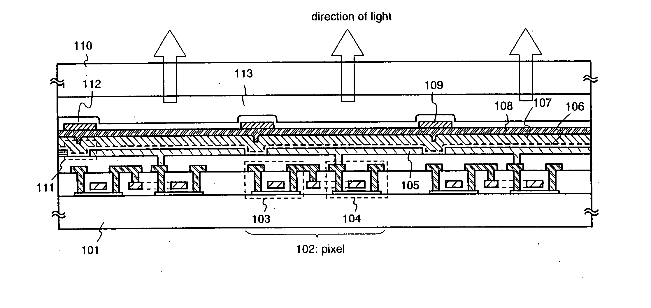
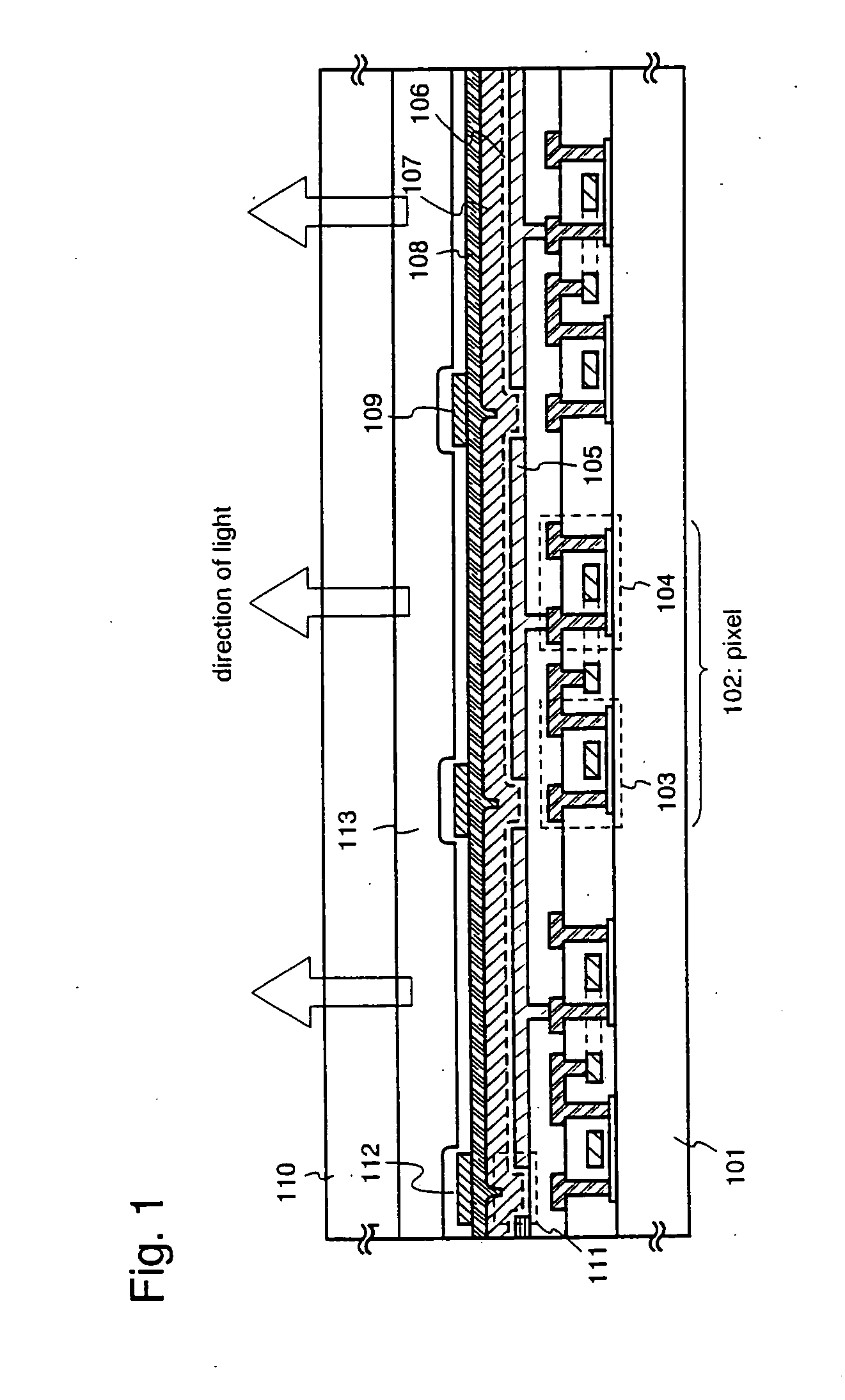
[0167]FIG. 3B shows that the amount of the off current value in the switching TFT in the pixel of the EL display device is reduced by using a multi-gate structure for the switching TFT, and the need for a storage capacitor is eliminated. However, it is also acceptable to make a structure of disposing a storage capacitor as is done conventionally. In this case, as shown in FIG. 12, a storage capacitor 1301 is formed in parallel to the gate of the current controlling TFT 202 with respect to the drain of the switching TFT 201.
[0168] Note that the constitution of embodiment 3 can be freely combined with any constitution of embodiments 1 and 2. Namely, a storage capacitor is merely formed within a pixel and it is not to limit the TFT structure, materials of EL layer, etc.
PUM
 Abstract
Description
Claims
Application Information
 - R&D
- Intellectual Property
- Life Sciences
- Materials
- Tech Scout
- Unparalleled Data Quality
- Higher Quality Content
- 60% Fewer Hallucinations
Browse by: Latest US Patents, China's latest patents, Technical Efficacy Thesaurus, Application Domain, Technology Topic, Popular Technical Reports.
© 2025 PatSnap. All rights reserved.Legal|Privacy policy|Modern Slavery Act Transparency Statement|Sitemap|About US| Contact US: help@patsnap.com