Capacitively coupled pulsed signaling bus interface

a pulsed signaling and bus interface technology, applied in pulse techniques, instruments, baseband system details, etc., can solve the problems of increasing signaling power consumption, difficult integration of a large number of high-speed i/os on a single chip, and low signaling power of parallel multi-drop or multi-point buses, etc., to achieve low power, reduce i/o signaling power, and increase the available channel bandwidth

Inactive Publication Date: 2006-12-28
RGT UNIV OF CALIFORNIA
View PDF7 Cites 34 Cited by
  • Summary
  • Abstract
  • Description
  • Claims
  • Application Information

AI Technical Summary

Benefits of technology

[0033] The present invention discloses novel circuit techniques [12] that reduce the I/O signaling power by a factor of 7.5 and increase the available channel bandwidth of a multi-point bus by a factor of 2 compared to the most recent memory bus I/O schemes. The proposed CCBI scheme, which incorporates differential bidirectional pulsed signaling, achieves 1 Gb/s over 10-cm printed circuit board traces with 2.9 mW of power for the driver and channel termination and 2.7 mW for the receiver pre-amplifier. To achieve this low power and high sig...

Problems solved by technology

Although the CMOS high-speed serial links already entered multi-Gb/s/pin speeds by using point-to-point connections and complicated equalization techniques [1], the speed of a parallel multi-drop or multi-point bus (e.g. memory interfaces) is still in less than 2 Gb/s/pin due to the signal integrity issues in a bandwidth limited printed circuit board (PCB) environment [2].
Also, the signaling power consumption is of increasing concern.
Integrating a large number of high-speed I/Os on a single chip becomes extremely challenging due to excessive complexity and power consumption.
In conventional bus-based systems with directly coupled multi-point connections, the available channel bandwidth has been primarily limited by the ISI resulting from the impedance discontinuities created by the transmission line stubs and multiple device capacitive loadings.
However, widely parallel serial-links have overhead in terms of large area, cost, and difficulty in system scaling.
In order to use this parallel bus topology for one more decade or even more, the problem remains how to increase the available bandwidth of a multi-point bus, how to achieve high signal integrity, and how to decrease the signaling power.
However, [6] requires the ISI subtraction time, which increases the receiver latency and limits the data rate.
A feed-forward equalizer [7] increases the I/O input capacitance, which may degrade the channel characteristics due to the complicated demultiplexing structure.
Thus these receiver equalization schemes are not simple and cost-effective for multi-Gb/s parallel bus I/Os.
However, [8] consumes large I/O power of 40 mW/pair, since the motherboard bus is driven by convention...

Method used


Image

  • Capacitively coupled pulsed signaling bus interface
  • Capacitively coupled pulsed signaling bus interface
  • Capacitively coupled pulsed signaling bus interface

Examples


Embodiment Construction

[0047] In the following description of a preferred embodiment, reference is made to the accompanying drawings, which form a part hereof, and in which is shown by way of illustration a specific embodiment in which the invention may be practiced. It is to be understood that other embodiments may be utilized and structural changes may be made without departing from the scope of the present invention.

[0048] Overview

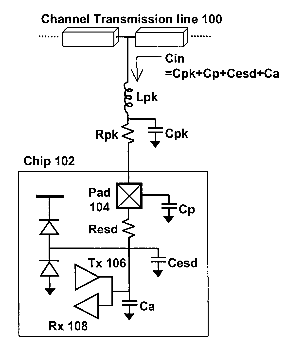
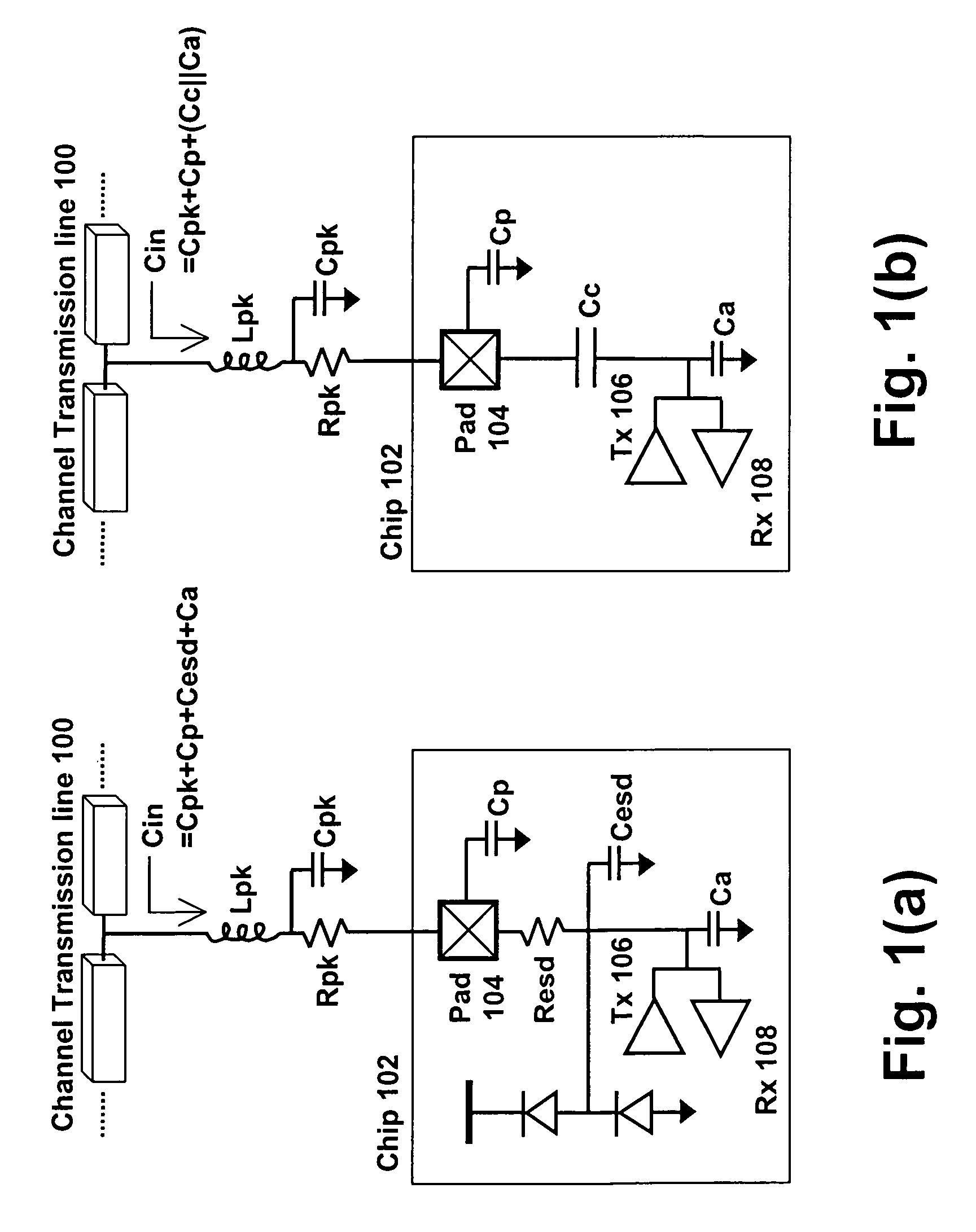
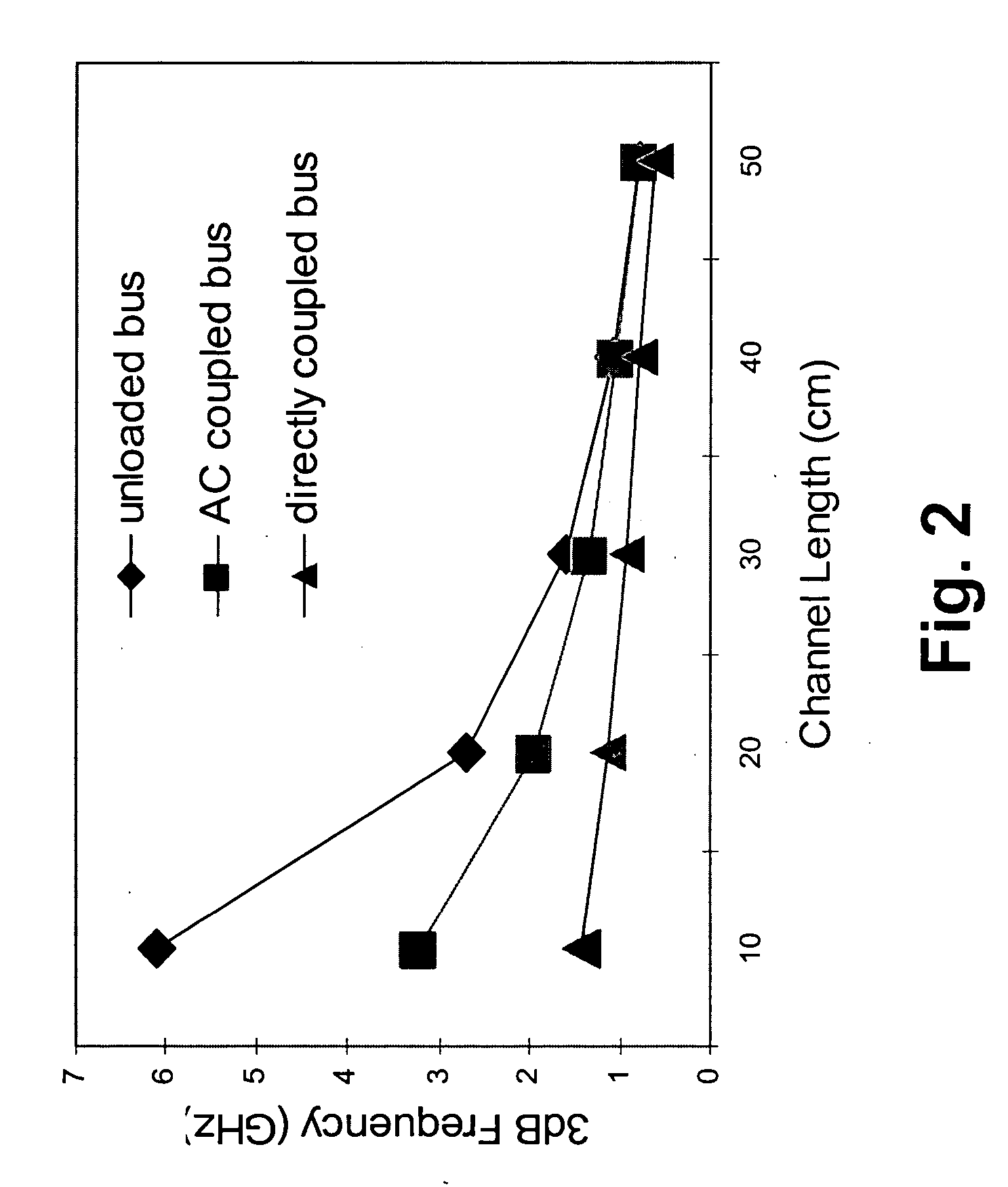
[0049] A new capacitive coupled pulsed signaling bus interface (CCBI) has been developed as an effective solution to reduce the I / O signaling power and improve the signal integrity in low-cost multi-point or multi-drop or point-to-point parallel bus systems. A single ended or differential synchronous pulsed signaling I / O technology utilizing on-chip capacitive coupling for low power, high bandwidth, parallel bus links (such as a system bus or a main memory bus) has been proposed.

[0050] Capacitive Coupled Pulsed Signaling Bus Interface (CCBI) System Architecture and Interco...


PUM


Abstract

A fully alternating current (AC) coupled multi-point, multi-drop or point-to-point bus interconnect uses a low power synchronous pulsed signaling scheme for board-level chip-to-chip communication. A single-ended or differential pulsed signaling transceiver generates a diamond data eye with a small time constant in the pulsed signal. The transceiver includes a high-pass filter or a differentiator circuit network that generates triangle pulses that make the diamond data eye.

Description

CROSS-REFERENCE TO RELATED APPLICATIONS [0001] This application is related to the following co-pending and commonly-assigned application: [0002] U.S. Provisional Patent Application Ser. No. 60 / 685,859, filed on May 31, 2005, by Jongsun Kim, Ingrid Verbauwhede, and Mau-Chung F. Chang, entitled “CAPACITIVELY COUPLED PULSED SIGNALING BUS INTERFACE,” attorneys docket number 30435.171-US-P1 (2005-352-1); [0003] which application is incorporated by reference herein.STATEMENT REGARDING FEDERALLY SPONSORED RESEARCH AND DEVELOPMENT [0004] This invention was made with Government support under Grant No. 0098361, awarded by the NSF. The Government has certain rights in this invention.BACKGROUND OF THE INVENTION [0005] 1. Field of the Invention. [0006] (Note: This application references to various publications as indicated in the specification by reference numbers enclosed in brackets, e.g., [x]. A list of these publications ordered according to these reference numbers can be found below in the ...

Claims


Application Information

Patent Timeline
IPC IPC(8): H03K17/16
CPCG06F13/4072Y02B60/1235Y02B60/1228H04L25/0266H01L2224/16225H01L2924/13091H01L2224/04042Y02D10/00H01L2224/4813H01L2924/00
Inventor KIM, JONGSUNVERBAUWHEDE, INGRIDCHANG, MAU-CHUNG F.
Owner RGT UNIV OF CALIFORNIA
Why Eureka
Try Eureka