Semiconductor device and manufacturing method of the same

a technology of semiconductors and manufacturing methods, applied in the direction of semiconductor devices, basic electric elements, electrical equipment, etc., can solve the problems of increasing complicated manufacturing process, so as to increase the manufacturing cost, and increase the number of steps

Inactive Publication Date: 2007-01-04
SEMICON ENERGY LAB CO LTD
View PDF13 Cites 49 Cited by
  • Summary
  • Abstract
  • Description
  • Claims
  • Application Information

AI Technical Summary

Benefits of technology

[0015] Conventionally, when various circuits are to be formed over the same substrate and a TFT with a structure suitable for each circuit is to be formed, there has been a problem in that the manufacturing process becomes complicated and the number of steps increases. It is clear that the increase in the number of steps is not only a factor in increasing manufacturing cost, but also a cause of reducing manufacturing yield.

Problems solved by technology

Conventionally, when various circuits are to be formed over the same substrate and a TFT with a structure suitable for each circuit is to be formed, there has been a problem in that the manufacturing process becomes complicated and the number of steps increases.
It is clear that the increase in the number of steps is not only a factor in increasing manufacturing cost, but also a cause of reducing manufacturing yield.
Further, in the technology disclosed in Patent Document 2, the LDD region is formed in a self-aligned manner, however, respective widths of the LDD regions disposed with the channel forming region interposed therebetween are equal, and it is difficult to control the width in accordance with each circuit.

Method used


Image

  • Semiconductor device and manufacturing method of the same
  • Semiconductor device and manufacturing method of the same
  • Semiconductor device and manufacturing method of the same

Examples


embodiment mode 1

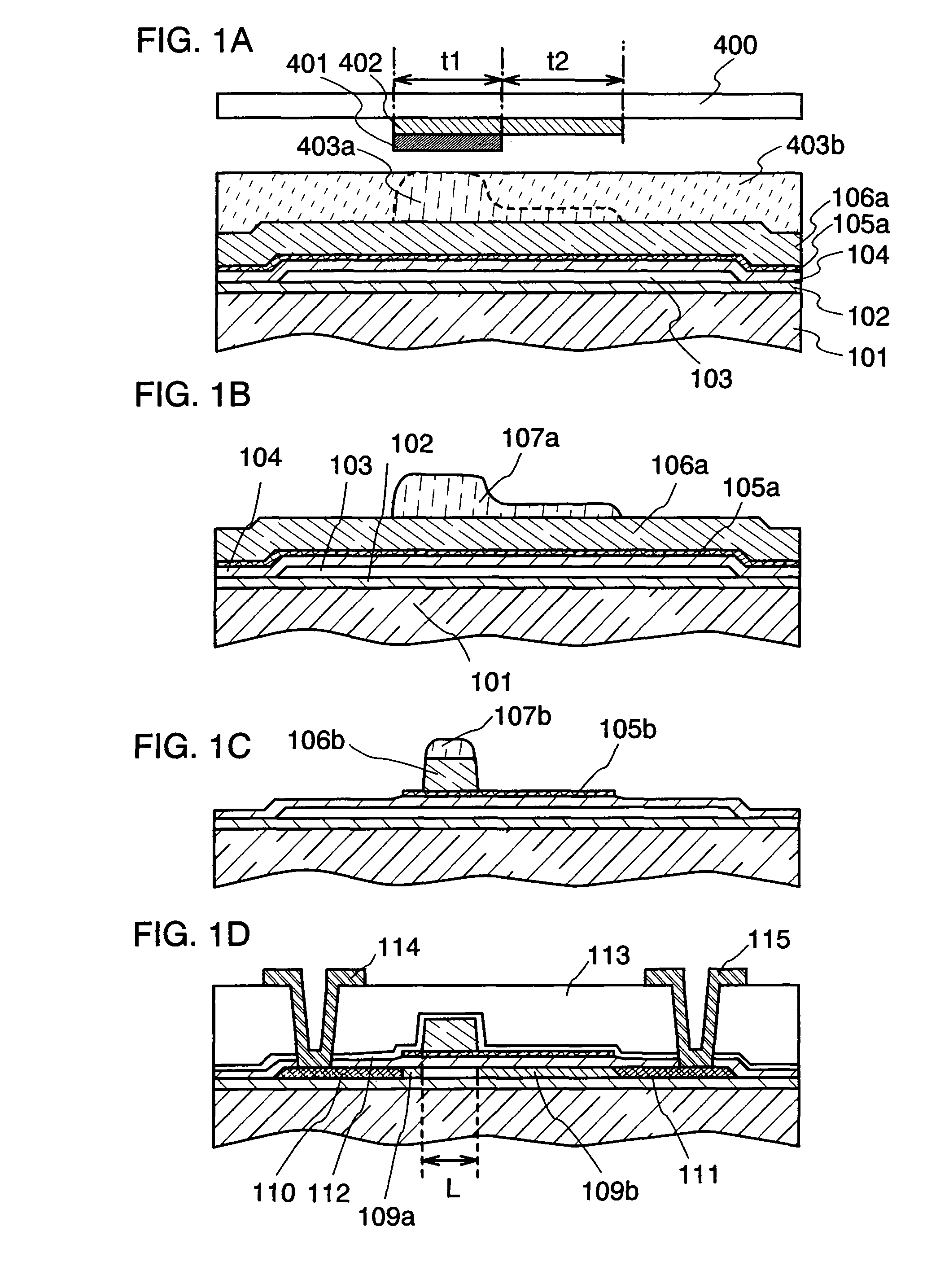
[0052] This embodiment mode describes a process for forming low-concentration impurity regions having different widths respectively on both sides of a channel forming region in a self-aligned manner by using a gate electrode of a TFT as a mask in ion-doping.

[0053] First, a first insulating film (a base insulating film) 102 is formed over a substrate 101 having an insulating surface. As the substrate 101 having an insulating surface, a light-transmitting substrate such as a glass substrate, a crystallized glass substrate, or a plastic substrate can be used. In the case where a thin film transistor to be formed is applied to a top emission light-emitting display device or a reflective liquid crystal display device, a ceramic substrate, a semiconductor substrate, a metal substrate, or the like can also be used.

[0054] As the first insulating film 102, a single layer or a stacked-layer of an insulating film such as a silicon oxide film, a silicon nitride film, or a silicon oxynitride (...

embodiment mode 2

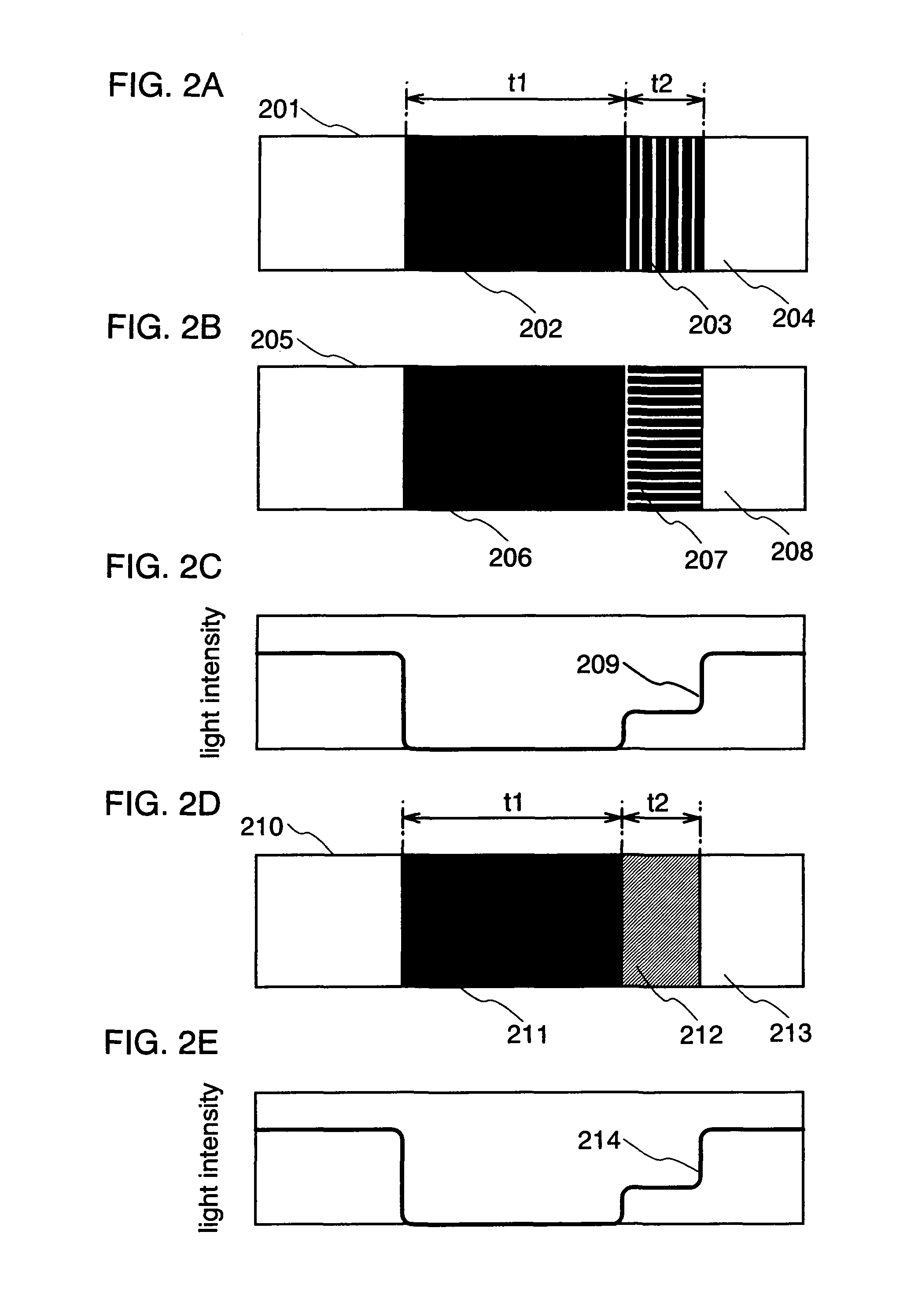
[0103] In this embodiment mode, an exposure mask provided with an auxiliary pattern having a light intensity reduction function formed of a diffraction grating pattern or a semi-transparent film, which is used in Embodiment Mode 1, is described with reference to FIGS. 2A to 2E.

[0104] Note that FIG. 1A is a cross-sectional view of an exposure mask. Similarly, also in FIGS. 2A to 2E, the width of a light shielding portion is denoted by t1 and the width of a portion provided with an auxiliary pattern is denoted by t2.

[0105] As specific examples of the auxiliary pattern, FIGS. 2A and 2B show part of top-plane views of an exposure mask provided with a diffraction grating pattern having a slit portion formed of a line and a space at or below the resolution limit of an exposure apparatus. Diffraction grating pattern is a pattern in which at least one pattern of a slit, a dot, or the like is provided. In the case where a plurality of patterns of a slit, a dot, or the like is provided, the...

embodiment mode 3

[0112] A method for forming the conductive stacked-layer pattern described in Embodiment Mode 1 is not particularly limited. Here, an example of forming a conductive stacked-layer pattern by changing the etching condition several times during a process is described with reference to FIGS. 3A to 3F.

[0113] First, similarly to Embodiment Mode 1, a resist pattern 307a is formed over a second conductive layer 306a. FIG. 3A corresponds to FIG. 1B.

[0114] Note that in FIG. 3A, over a substrate 301, a first insulating film (base insulating film) 302, a semiconductor layer 303, and a second insulating film (gate insulating film) 304 are formed, and over that, a first conductive layer 305a and the second conductive layer 306a are formed.

[0115] Then, etching is performed in a first etching condition so that the resist pattern 307b and the second conductive layer 306b are formed with a shape shown in FIG. 3B. A tapered portion is formed in a part of the second conductive layer 306b in the fir...


PUM


Abstract

To provide a manufacturing method in which LDD regions with different widths are formed in a self-aligned manner, and the respective widths are precisely controlled in accordance with each circuit. By using a photomask or a reticle provided with an auxiliary pattern having a light intensity reduction function formed of a diffraction grating pattern or a semi-transparent film, the width of a region with a small thickness of a gate electrode can be freely set, and the widths of two LDD regions capable of being formed in a self-aligned manner with the gate electrode as a mask can be different in accordance with each circuit. In one TFT, both of two LDD regions with different widths overlap a gate electrode.

Description

BACKGROUND OF THE INVENTION [0001] 1. Field of the Invention [0002] The present invention relates to a semiconductor device having a circuit constituted by a thin film transistor (hereinafter referred to as a “TFT”) and a manufacturing method of the same. For example, the invention relates to electronic equipment on which an electro-optical device typified by a liquid crystal display panel or a light emitting display device having an organic light-emitting element (or an inorganic light-emitting element) is mounted as a component. [0003] In this specification, ‘semiconductor device’ means any device that can function by utilizing semiconducting properties, and electro-optical devices, semiconductor circuits and electronic equipment are all included in the semiconductor device. [0004] 2. Description of the Related Art [0005] In recent years, a technique for forming a thin film transistor (TFT) by using a semiconductor thin film (with a thickness of about several nm to several hundred...

Claims


Application Information

Patent Timeline
Patent Type & Authority Applications(United States)
IPC IPC(8): H01L21/84H01L27/12
CPCH01L27/1214H01L27/1288H01L29/78624H01L27/124H01L27/127H01L29/42384
Inventor OHNUMA, HIDETOMONOE, SHIGEHARU
Owner SEMICON ENERGY LAB CO LTD
Why Eureka
Try Eureka