

Method of manufacturing wiring substrate, and wiring substrate
a manufacturing method and technology of wiring substrate, applied in the direction of resistive material coating, metallic material coating process, pretreatment surface, etc., can solve the problems of inability to use such a substance, difficulty in achieving high accuracy of very fine regions (very fine wires), etc., to improve bonding strength, improve adhesion, and improve thermal resistance.
- Summary
- Abstract
- Description
- Claims
- Application Information
AI Technical Summary
Benefits of technology
Problems solved by technology
Method used
Image

Examples
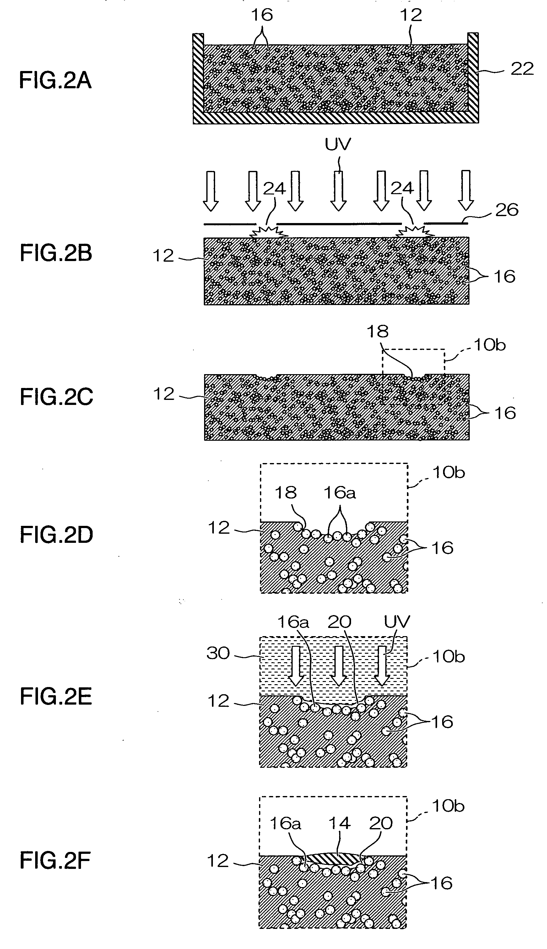
first embodiment
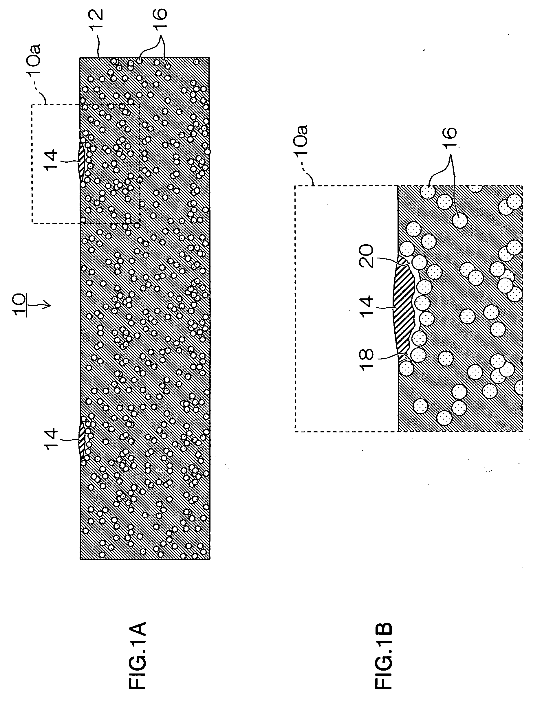
[0044]FIG. 1 is a cross-sectional diagram showing the approximate composition (three-dimensional structure) of a wiring substrate 10 relating to a wiring substrate and a method of manufacturing a wiring substrate according to the present invention. FIG. 1B is an enlarged diagram of the portion indicated by the dotted line 10a in FIG. 1A.
[0045] The wiring substrate 10 according to the present embodiment has a structure in which conducting layers 14 forming wires are formed on a resin layer 12.
[0046] The resin layer 12 has a composition in which photocatalyst particles 16 having a photocatalyst function are contained in a resin material which acts as a filler that serves to improve strength and reduce thermal expansivity. Although the details of the photocatalyst particles 16 are described hereinafter, these photocatalyst particles 16 are contained at a rate of approximately 30 to 70% (percentage by weight) with respect to the resin layer 12.
[0047] As shown in detail in FIG. 1B, a ...
second embodiment
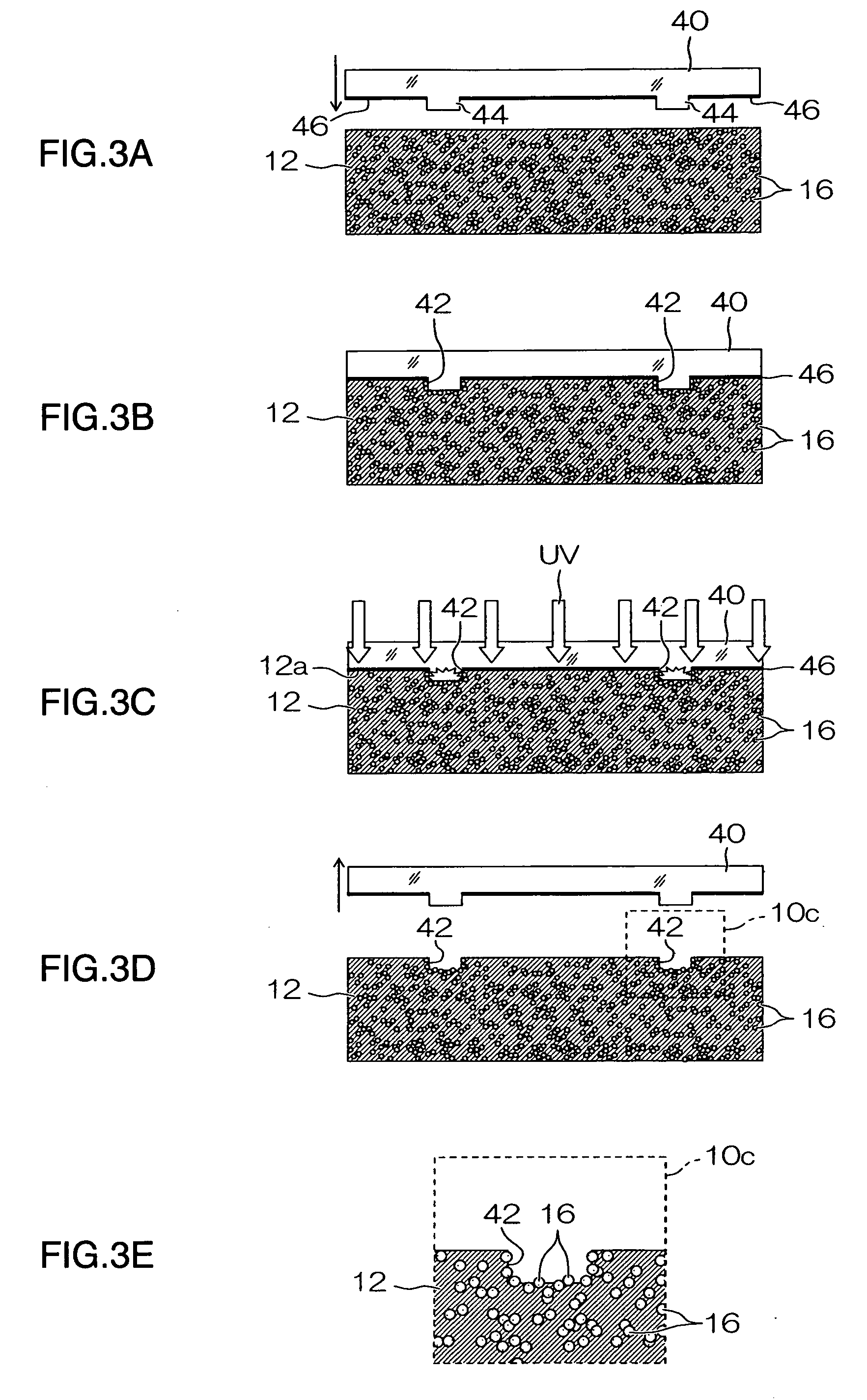
[0061] Next, a second embodiment of the present invention is described below. In the second embodiment, of the steps of manufacturing the wiring substrate, the photocatalyst particle exposure step is different to that of the first embodiment described above. In the second embodiment, items which are the same as or similar to those in the first embodiment described above are labeled with the same reference numerals and description thereof is omitted here. FIGS. 3A to 3E show schematic views of a photocatalyst particle exposure step according to the second embodiment.
[0062] In the photocatalyst particle exposure step shown in FIGS. 3A to 3E, in the pattern groove formation step shown in FIGS. 3A and 3B, pattern grooves are formed in the resin layer 12 by using a mold (stamper) 40.
[0063] This mold40 is made from a material which transmits ultraviolet light, such as quartz, and projecting sections 44 corresponding to desired wiring patterns (in other words, projecting sections 44 havi...
third embodiment
[0072] Next, a third embodiment of the present invention is described below. In the third embodiment, items which are the same as or similar to those in the first embodiment or second embodiment described above are labeled with the same reference numerals and description thereof is omitted here.
[0073] In the photocatalyst particle exposure step shown in FIGS. 4A to 4C, the photocatalyst particles 16 are exposed by means of a photocatalytic reaction based on irradiation of laser light. In other words, a laser is irradiated in a pattern shape on the resin layer 12 as shown in FIG. 4B. After that, as shown in FIG. 4C, the resin layer 12 is removed by a photocatalytic reaction using irradiation of laser light, thereby patterns 50 being formed, and at the same time, the photocatalyst particles 16 in the sections of the resin layer 12 irradiated with laser light become exposed at the surface of the resin layer 12. Since the patterns 50 are formed by laser light, it is possible to obtain ...
PUM
| Property | Measurement | Unit |
|---|---|---|
| width | aaaaa | aaaaa |
| wavelength | aaaaa | aaaaa |
| thickness | aaaaa | aaaaa |
Abstract
Description
Claims
Application Information