Electroluminescence device, method of manufacturing electroluminescence device, and electronic apparatus

a technology of electroluminescence device and electroluminescence device, which is applied in the manufacture of electrode systems, electric discharge tubes/lamps, and discharge tubes luminescent screens, etc., can solve the problems of low reflection layer, low production efficiency, and low production efficiency, and achieve high display performance, easy formation of anodes, and high precision

Active Publication Date: 2007-01-18
SEIKO EPSON CORP
View PDF16 Cites 114 Cited by
  • Summary
  • Abstract
  • Description
  • Claims
  • Application Information

AI Technical Summary

Benefits of technology

[0012] An advantage of the invention is to provide an electroluminescence device which can prevent a lower reflection layer of an optical resonator located below an anode from deteriorating when the film thickness of the anode is caused to be different for each of a plurality of pixels, a method of manufacturing the electroluminescence device, and an electronic apparatus.
[0013] Another advantage of the invention is to provide an electroluminescence device which can easily form an anode with high precision by a small number of steps to realize high display performance and low cost when the film thickness of the anode is caused to be different for each of a plurality of pixels, a method of manufacturing the electroluminescence device, and an electronic apparatus.
[0014] According to an aspect of the invention, there is provided a method of manufacturing an electroluminescence device, in which a plurality of pixel forming regions is formed on a substrate, a light emitting element, in which an anode having a light transmission property, a light emission function layer including at least a light emitting layer and a cathode are laminated, is provided in each of the plurality of pixel forming regions, the pixel forming regions include a pixel forming region of first color and a pixel forming region of second color different from the first color, and the anode includes a first anode formed in the pixel forming region of the first color with a first thickness g and a second anode formed in the pixel forming region of the second color with a second thickness b, including: forming a first transparent conductive film in the pixel forming region of the first color with a thickness g−b obtained by subtracting the second thickness b from the first thickness g; and forming a second transparent conductive film in the pixel forming region of the second color with the second thickness b.
[0015] According to the invention, for example, in an electroluminescence device for displaying two primary colors (for example, green and blue), it is possible to easily realize an anode having an optical film thickness (optical length or optical distance) which is optimal in optical resonance of each color.
[0016] Here, a case where an anode having a first thickness dr is formed in a red pixel forming region and an anode having a second thickness dg is formed in a green pixel forming region will be described. First, in a first step, an anode having a thickness of dr−dg is formed in the red pixel forming region. Next, in a second step, an anode having the second thickness dg is laminated in the red pixel forming region and, at the same time, the anode having the second thickness dg is formed in the green pixel region. Then, the anode having a thickness (dr−dg+dg)=dr is formed in the red pixel forming region and the anode having a thickness dg is formed in the green pixel forming region.
[0017] In this case, for example, the first thickness dr may be twice the second thickness dg and the thicknesses of the anodes formed in the respective steps may be identical to each other. Therefore, according to the invention, the etching times of the first step and the second step may be similar to each other. According to the invention, it is possible to suppress the number of photolithographic processes from increasing, to prevent a side edge from being generated due to long-time etching, and to facilitate process management. In the invention, the pixel represents a light emitting element and a light emitting part (light emitting region) in which the light emitting element is formed and a pixel group is a set of pixels which emits different color light or same color light.

Problems solved by technology

As a result, the lower reflection layer is etched by etchant or etching gas used for etching the ITO film and thus the reflection property of the lower reflection layer deteriorates or lack of the lower reflection layer is caused.
When the etching time varies depending on the step, it is difficult to manage the process.
Since the ITO film is formed by plural steps, the steps become complicated and thus productivity deteriorates.
Accordingly, it is difficult to form the thin anode with high precision and thus the thickness precision of the anode deteriorates.

Method used


Image

  • Electroluminescence device, method of manufacturing electroluminescence device, and electronic apparatus
  • Electroluminescence device, method of manufacturing electroluminescence device, and electronic apparatus
  • Electroluminescence device, method of manufacturing electroluminescence device, and electronic apparatus

Examples


first embodiment

Basic Configuration of EL Device

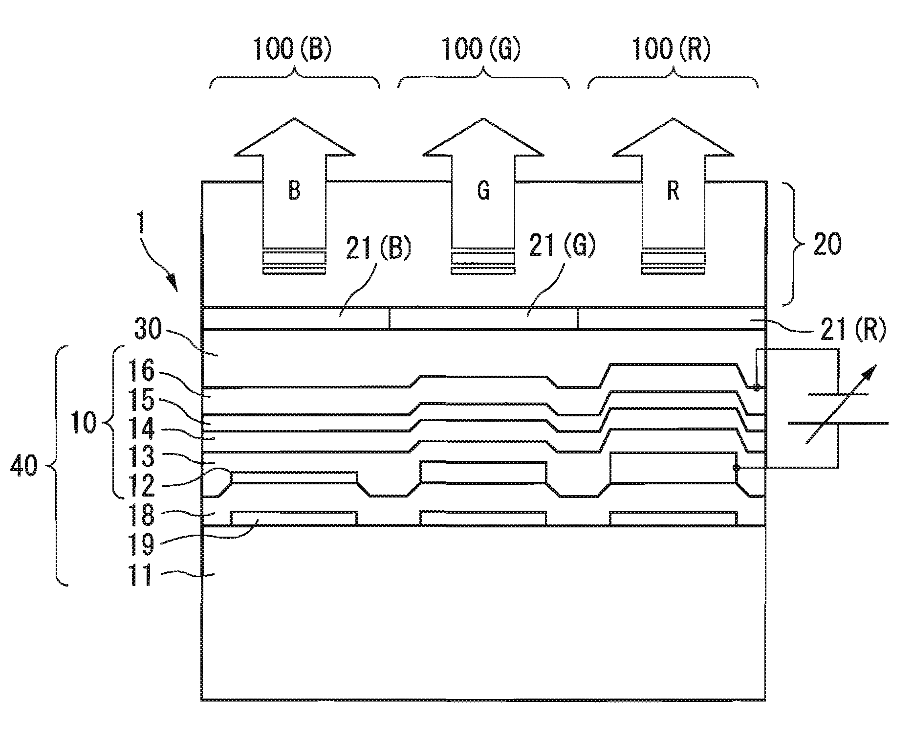
[0101]FIG. 1 is a cross-sectional view schematically showing a configuration of an organic EL device (EL device) according to a first embodiment of the invention.

[0102] In FIG. 1, an organic EL device 1 according to the present embodiment is a too emission type device for emitting display light toward the opposite side of a substrate 11 when viewed from a light emitting layer 14. The organic EL device 1 has pixels 100(R), 100(G) and 100(B). The pixel 100(R) emits red (R) light, the pixel 100(G) emits green (G) light, and the pixel 100(B) emits blue (B) light. In the pixels 100(R), 100(G) and 100(B), an organic EL element 10 is formed.

[0103] The organic EL element 10 has a transparent anode 12 formed of indium tin oxide (ITO), a hole transport layer 13, a light emitting layer 14, an electron transport layer 15, and a cathode layer 16 formed of magnesium-silver alloy and having semitransparent reflectivity, all of which are laminated on the substrat...

second embodiment

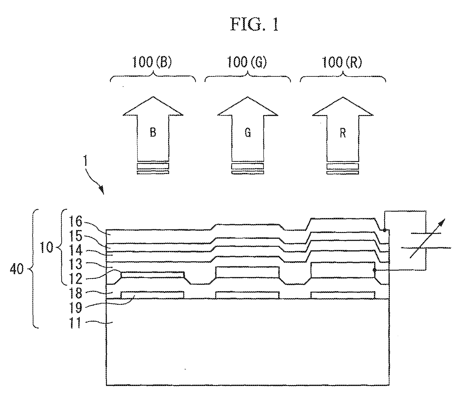
[0147]FIG. 4 is a cross-sectional view schematically showing a configuration of an organic EL device (EL device) according to a second embodiment of the invention.

[0148] The organic EL device 1 shown in FIG. 4 is a top emission type device for emitting display light toward the opposite side of a substrate 11 when viewed from a light emitting layer 14. In the pixel 100(R) for emitting red (R) light, the pixel 100(G) for emitting green (G) light, the pixel 100(B) for emitting blue (B) light, an organic EL element 10 is formed. The organic EL element 10 has a transparent anode 12 formed of ITO, a hole transport layer 13, a light emitting layer 14, an electron transport layer 15, and a cathode layer 16 formed of magnesium-silver alloy and having semitransparent reflectivity, all of which are laminated on the substrate 11 formed of glass in that order.

[0149] A reflection layer 19 (total reflection layer) formed of aluminum, aluminum alloy, silver or silver alloy is formed between the s...

third embodiment

[0169] Next, an organic EL device (EL device) according to a third embodiment of the invention will be described.

[0170]FIG. 6 is a schematic diagram showing a wiring structure of an organic EL device according to the present embodiment. In FIG. 6, reference numeral 1 denotes the organic EL device.

[0171] The organic EL device 1 is an active matrix type using a thin film transistor (hereinafter, referred to as TFT) as a switching element, and has a wiring structure including a plurality of scan lines 101 . . . , a plurality of signal lines 102 . . . extending in a direction perpendicular to the scan lines 101, and a plurality of power source lines 103 . . . extending parallel to the signal lines 102. Pixels X . . . , are formed at the peripheries of intersections between the scan lines 101 . . . and the signal lines 102 . . . .

[0172] According to the technical spirit of the invention, the active matrix using the TFT is not necessarily required and a passive matrix substrate may be ...


PUM


Abstract

Provided is a method of manufacturing an electroluminescence device, in which a plurality of pixel forming regions is formed on a substrate, a light emitting element, in which an anode having a light transmission property, a light emission function layer including at least a light emitting layer and a cathode are laminated, is provided in each of the plurality of pixel forming regions, the pixel forming regions include a pixel forming region of first color and a pixel forming region of second color different from the first color, and the anode includes a first anode formed in the pixel forming region of the first color with a first thickness and a second anode formed in the pixel forming region of the second color with a second thickness, including: forming a first transparent conductive film in the pixel forming region of the first color with a thickness obtained by subtracting the second thickness from the first thickness; and forming a second transparent conductive film in the pixel forming region of the second color with the second thickness.

Description

[0001] The invention contains subject matter related to Japanese Patent Application 2005-206552 filed on Jul. 15, 2005 and Japanese Patent Application 2005-206708 filed on Jul. 15, 2005, in the Japanese Patent Office, the entire contents of which being incorporated herein by reference. BACKGROUND [0002] 1. Technical Field [0003] The present invention relates to an electroluminescence device, a method of manufacturing the electroluminescence device and an electronic apparatus. [0004] 2. Related Art [0005] As a display device used for an electronic apparatus such as a mobile phone, a personal computer or a personal digital assistant (PDA) or an exposure head in an image forming apparatus such as a digital copier or a printer, a light emitting device such as an organic electroluminescence device (hereinafter, abbreviated to organic EL device) is attracting much attention. [0006] Such a light emitting device, in order to realize color display, a configuration for emitting light of each ...

Claims


Application Information

Patent Timeline
IPC IPC(8): H01J9/24H01J1/62
CPCH01L27/3211H01L27/322H01L2251/558H01L51/5265H01L51/5206H10K59/35H10K59/38H10K2102/351H10K59/80517H10K59/80518H10K59/876H05B33/26H05B33/10H10K50/852H10K50/81H10K50/816H10K50/818
Inventor MAEDA, TSUYOSHIMATSUMOTO, TOMOTAKA
Owner SEIKO EPSON CORP
Why Eureka
Try Eureka