Semiconductor device and a method of manufacturing the same

a manufacturing technology and integrated circuit technology, applied in semiconductor devices, semiconductor/solid-state device details, electrical devices, etc., can solve the problems of difficult to completely fill the filler in the via hole, and the anti-reflective film cannot be formed uniformly over the interlayer insulating film, so as to simplify the formation step of dual damascene. , the effect of high yield

Active Publication Date: 2007-01-25
RENESAS ELECTRONICS CORP
View PDF4 Cites 28 Cited by
  • Summary
  • Abstract
  • Description
  • Claims
  • Application Information

AI Technical Summary

Benefits of technology

[0016] An object of the present invention is to provide a technology of forming a multilevel Cu interconnect in a high yield by the dual damascene process.
[0017] Another object of the present invention is to provide a technology capable of simplifying the formation step of a multilevel Cu interconnect by the dual damascene process.
[0022] The present invention enables to form a multilevel Cu interconnect in a high yield by the dual damascene process. In addition, the invention enables to simplify the dual damascene formation step of a multilevel Cu interconnect.

Problems solved by technology

When a via hole has greater diameter and depth, however, it becomes difficult to completely fill a filler in the via hole in the above-described Step 3.
As a result, when after deposition of a filler over an interlayer insulating film including the inside of a via hole, the filler outside of the via hole is removed by etch back, the surface of the filler filled in the via hole does not become flat and there appears a difference between the surface of the filler and the surface of the interlayer insulating film, leading to a problem that in Step 4, an antireflective film cannot be formed uniformly over the interlayer insulating film.

Method used


Image

  • Semiconductor device and a method of manufacturing the same
  • Semiconductor device and a method of manufacturing the same
  • Semiconductor device and a method of manufacturing the same

Examples


embodiment 1

(Embodiment 1)

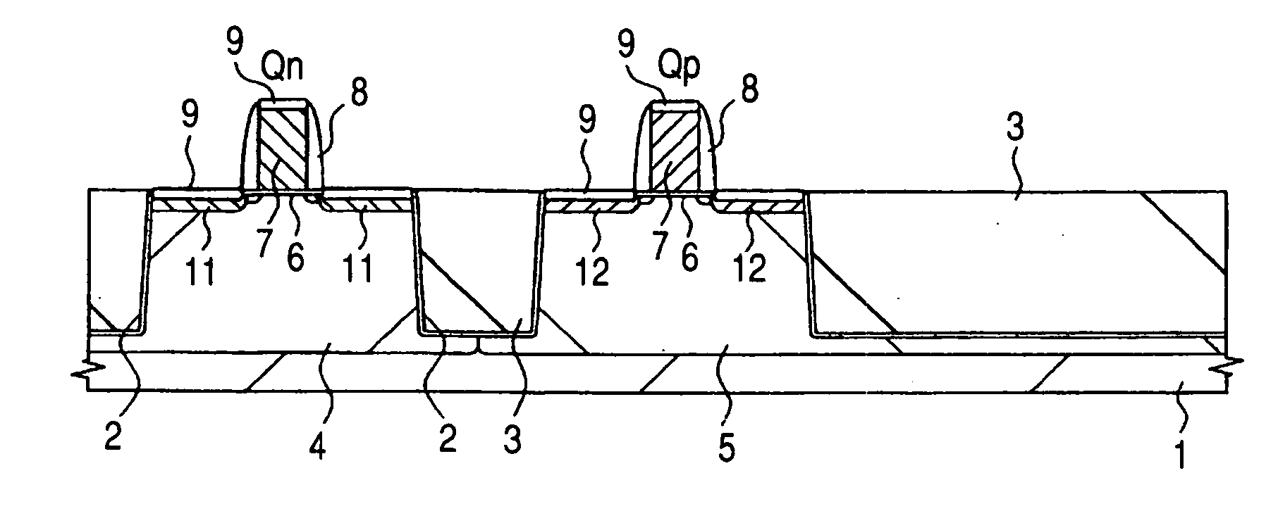
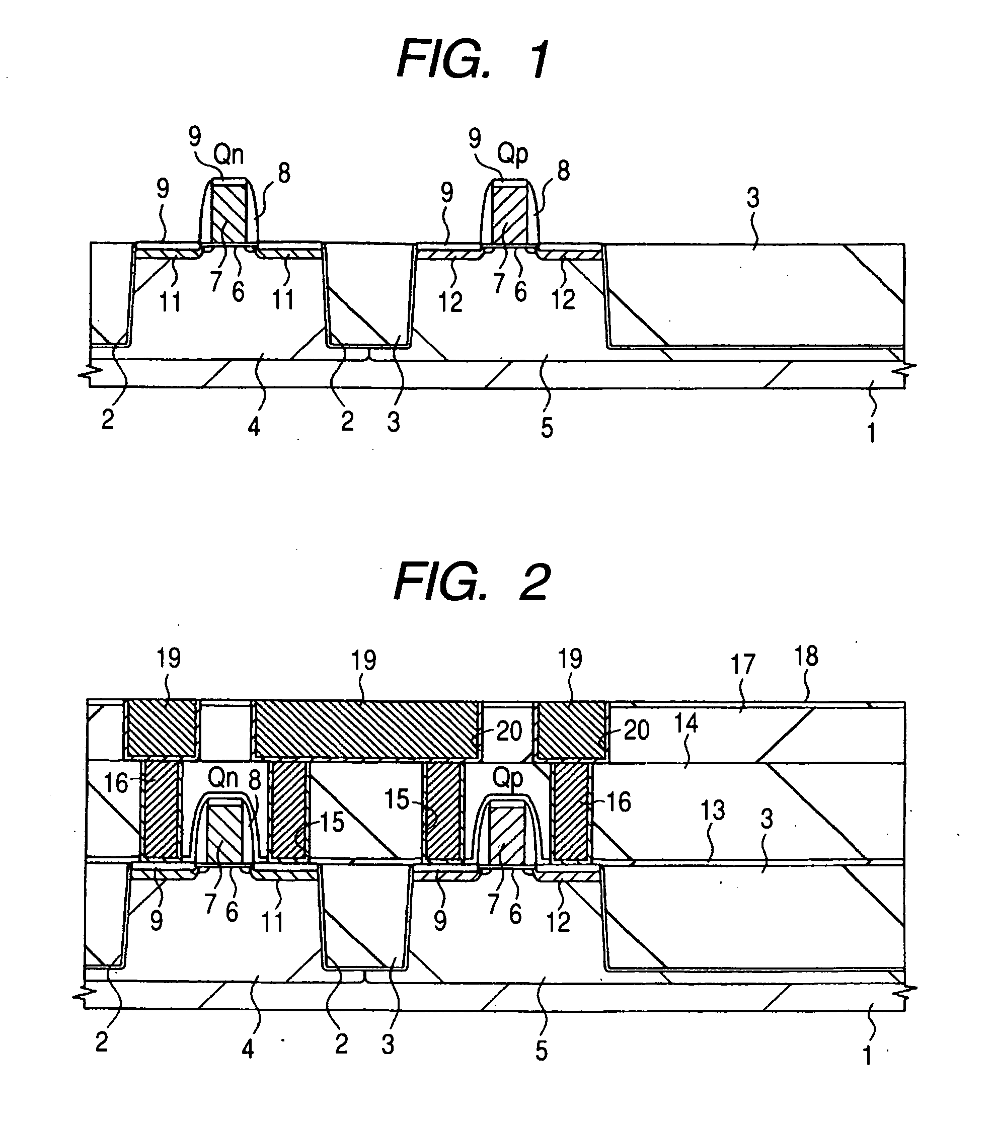
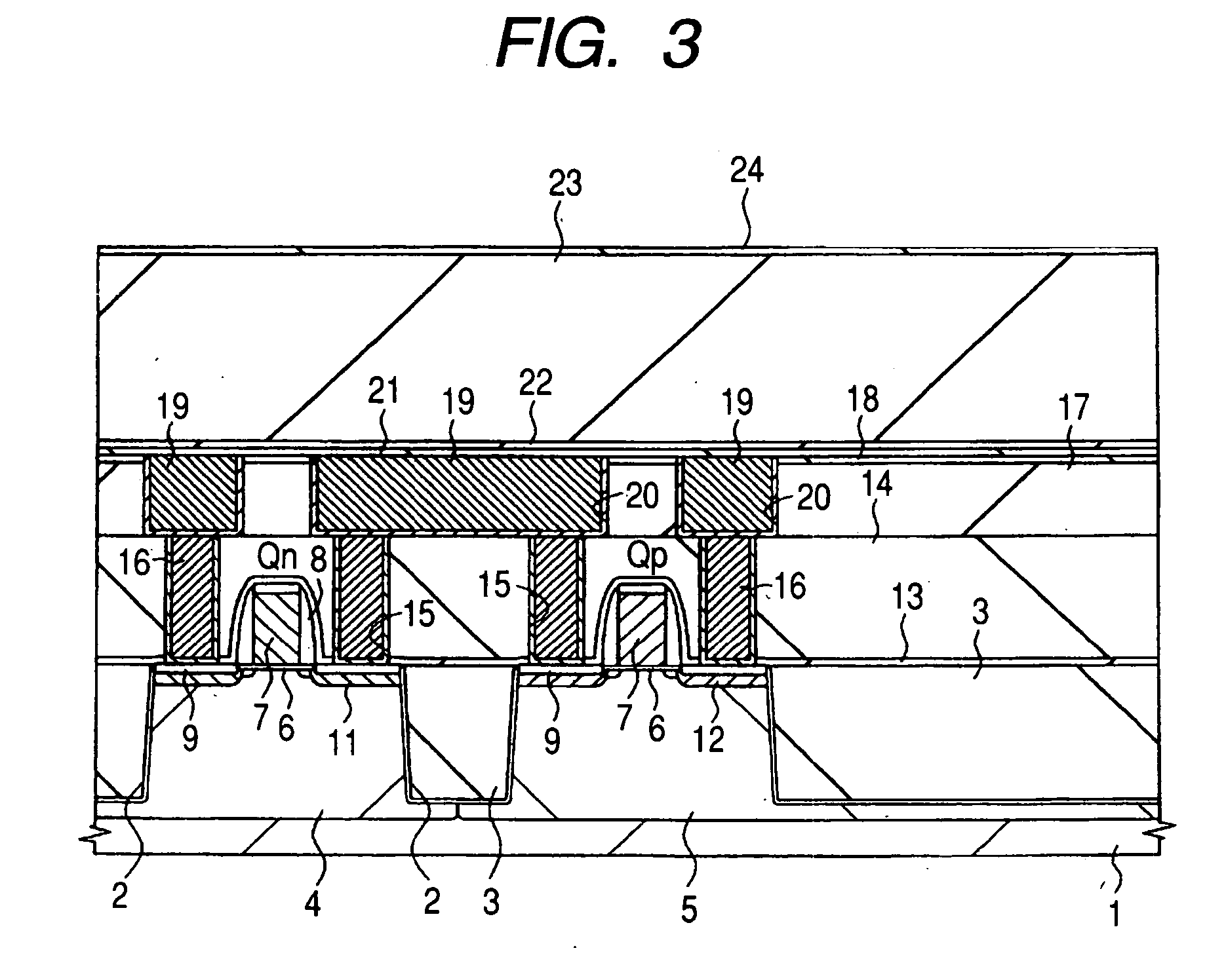
[0054] A semiconductor integrated circuit device having, for example, a four-layer Cu interconnect and fuse will be described in this Embodiment. A manufacturing method of it will next be described in the order of steps referring to FIGS. 1 to 26.

[0055] As illustrated in FIG. 1, an n channel MISFET (Qn) and a p channel MISFET (Qp) are formed as semiconductor elements over the main surface of a semiconductor substrate (which will hereinafter be called “substrate” simply), for example, made of single crystal silicon. In this drawing, indicated at numerals 2, 4 and 5 are element isolation trench, p well and n well, respectively.

[0056] The element isolation trench 2 is formed by filling an insulating film, for example, a silicon oxide film 3 in a trench formed by etching the substrate 1. The p well 4 and n well 5 are formed by ion-implanting p type impurity (boron) and n type impurity (phosphorus) into the substrate 1 and heat treating the substrate 1 to diffuse these im...

embodiment 2

(Embodiment 2)

[0101] In Embodiment 1, an interconnect trench was formed after formation of a via hole in an interlayer insulating film. In this Embodiment, on the other hand, a via hole is formed after formation of an interconnect trench in an interlayer insulating film.

[0102] As illustrated in FIG. 27, a barrier insulating film 44 and an interlayer insulating film 45 are deposited over a third-level interconnect 43. A stopper film 46 is formed in the interlayer insulating film 45. An SiCN film of from about 10 nm to 100 nm thick deposited by plasma CVD is used as the stopper film 46. Steps until this step are similar to those described referring to FIGS. 1 to 15 in Embodiment 1.

[0103] As illustrated in FIG. 28, after formation of a photoresist film 51 over the interlayer insulating film 45, the interlayer insulating film 45 is dry etched with the photoresist film 51 as a mask. By stopping etching at the surface of the stopper film 46, interconnect trenches 52 and 53 are formed in...


PUM


Abstract

For simplifying the dual-damascene formation steps of a multilevel Cu interconnect, a formation step of an antireflective film below a photoresist film is omitted. Described specifically, an interlayer insulating film is dry etched with a photoresist film formed thereover as a mask, and interconnect trenches are formed by terminating etching at the surface of a stopper film formed in the interlayer insulating film. The stopper film is made of an SiCN film having a low optical reflectance, thereby causing it to serve as an antireflective film when the photoresist film is exposed.

Description

CROSS-REFERENCE TO RELATED APPLICATION [0001] The present application claims priority from Japanese patent application No. 2005-197938 filed on Jul. 6, 2005, the content of which is hereby incorporated by reference into this application. BACKGROUND OF THE INVENTION [0002] The present invention relates to a manufacturing technology of a semiconductor integrated circuit device, in particular, a technology effective when applied to the formation of interconnects using the dual damascene process. [0003] In recent years, a fine-pitch interconnect forming method called damascene process is becoming a leading method in the manufacture of a miniaturized semiconductor integrated circuit device. [0004] The damascene process involves forming a fine interconnect trench in an interlayer insulating film over a semiconductor substrate, depositing a metal film over the interlayer insulating film including the inside of this interconnect trench, removing the metal film outside the interconnect trenc...

Claims


Application Information

Patent Timeline
Patent Type & Authority Applications(United States)
IPC IPC(8): H01L21/338
CPCH01L21/76808H01L21/76832H01L2924/1306H01L21/76834H01L21/823871H01L23/5258H01L23/53238H01L23/53295H01L24/11H01L2224/13099H01L2924/01004H01L2924/01005H01L2924/01013H01L2924/01015H01L2924/01022H01L2924/01027H01L2924/01029H01L2924/01033H01L2924/01047H01L2924/01073H01L2924/01074H01L2924/01078H01L2924/01079H01L2924/01082H01L2924/04941H01L2924/04953H01L2924/14H01L2924/19043H01L2924/30105H01L2924/01006H01L2924/01019H01L2924/014H01L21/76841H01L21/76895H01L2924/00H01L2924/12042H01L21/28H01L23/5226H01L23/5283H01L23/528H01L23/53209H01L23/5329H01L21/76811H01L21/823475
Inventor HOTTA, KATSUHIKOSASAHARA, KYOKO
Owner RENESAS ELECTRONICS CORP
Why Eureka
Try Eureka