Digital design component with scan clock generation

a digital design and clock generation technology, applied in the field of flip-flop design elements and scan clock generation therefor, can solve the problems of consuming one gate delay budget of critical path gate delay, affecting the operation frequency of a chip, and increasing the critical data path delay of functional mode data, so as to reduce the noise generated and critical path delay, reduce the area consumed by the chip, and eliminate the violation of scan mode hold

Active Publication Date: 2007-01-25
TEXAS INSTR INC
View PDF7 Cites 42 Cited by
  • Summary
  • Abstract
  • Description
  • Claims
  • Application Information

AI Technical Summary

Benefits of technology

[0020] In accordance with the present invention, a flip-flop architecture with scan mode functionality eliminates scan mode hold violations and reduces chip area consumed, power consumed, noise generated and critical path delays for application architectures using the flip-flop design. The elimination of hold violations in scan mode permits the removal or omission of scan mode path delay buffers. The separation of various functions according to different modes in the architecture permits scan mode logic and functional mode logic to be independent so that operation of one mode path does not induce toggling or power consumption in another mode path.
[0022] The slave stage of the flip-flop architecture is provided with a gated scan mode output to permit independent scan data propagation. Accordingly, the scan data output is not active during functional mode so that scan logic is not toggled during functional mode. The separate, non-overlapping clocks used during scan mode eliminate scan mode hold violations in the flip-flop scan chain. Accordingly, the flip-flop architecture of the present invention permits savings in circuit area through the omission of scan mode delay buffers. A main difference between the flip-flop architecture of the present invention and that of prior designs is the additional scan mode clock input used in the flip-flop design of the present invention. The provision of the additional clock to the flip-flop permits significant advantages in flip-flop architecture and overall system design, as discussed above, and in greater detail below. In addition, the scan mode clocks may be generated according to a number of techniques.

Problems solved by technology

The operating frequency of a chip is typically limited by intrinsic delays, setup times and tolerance variations in clock duty cycles.
First, multiplexer 11 may be viewed as increasing the critical data path delay of the functional mode data.
Second, multiplexer 11 may be viewed as consuming one gate delay of critical paths gate delay budget.
In addition, multiplexer 11 increases power consumed in functional mode when both the functional and scan data input toggle when the flip-flop changes logic states.
Another difficulty with latched based, edge triggered flip-flops is observed in the potential race conditions when the same the clock edge is used to both launch and capture data.
When the ΔTCLK—Q and ΔTsetup delay values are minimized to increase operating frequency, there is an increased probability that two back-to-back flops can experience data race-through problems.
In addition, clock skew between launching and capturing flops often creates and / or exacerbates hold time violations.
However, scan chain reordering has the potential to create a large set of scan mode hold violations, since scan data would then be routed to the closest possible flip-flop.
The shorter routes lead to less propagation delay which in turn lead to higher likelihood of scan mode hold violations.
While hold violations can occur in any functional operating mode of the circuit, the greatest number of violations typically occur during scan shift / capture modes.
The number of hold violations induced by scan chain reordering can be potentially enormous.
The drawbacks that typically occur with the insertion of delay buffers include additional usage of chip area, an increase in routing congestion, diminished signal integrity through increased cross talk and increased power consumption.
Any of these drawbacks also can trigger additional implementation or timing closure iterations that add to the implementation costs of the circuit.
The addition of a large number of hold buffers results in an increase in chip area.
Scan logic consumes a certain amount of power during normal functional mode operation, and circuit designs typically take into account routing and connectivity of scan logic paths and their impact on critical paths and operation of the normal functional mode logic.
The reused outputs often result in metal routing and buffers in the scan data path that create parasitic loads on the critical paths that can impact critical path delays in the circuit.
Such a technique is implementation sensitive and a ΔTCLK—Q delay may be difficult to avoid in the critical path of the flip-flop.

Method used


Image

  • Digital design component with scan clock generation
  • Digital design component with scan clock generation
  • Digital design component with scan clock generation

Examples


Embodiment Construction

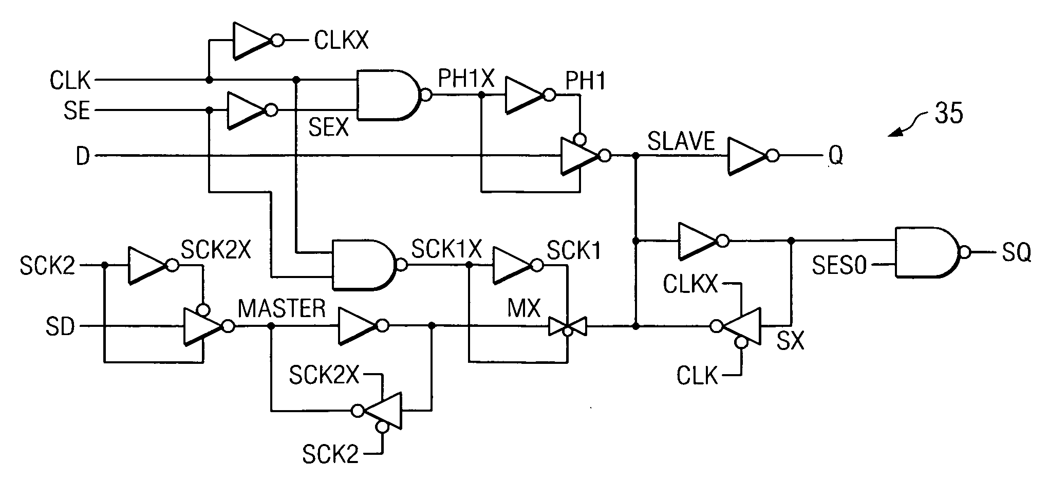
[0047] The present invention integrates the functionality of a scan mode multi-plexer into the structure of the flip-flop with non-overlapping scan mode clocks. The new flip-flop structure uses two non-overlapping clock signals during scan mode. The two clock signals can be generated according to a number of different techniques.

[0048] The scan mode flip-flop function previously realized as a two to one multiplexer and a single port latch, is obtained with a dual port latch with integrated clock gate, thereby providing a number of significant advantages. One particular advantage is that the novel flip-flop structure according to the present invention has many of the same features when viewed externally as previous muxed scan flip-flop elements so that it can be readily used in traditional tools and architectures. That is, the flip-flop maintains compatibility and portability with design tools. One difference is an additional scan mode clock provided to the flip-flop, which can be r...


PUM


Abstract

A master and a slave stage of a flip-flop are each separately clocked with non-overlapping clock signals during scan mode to eliminate a data input scan mode multiplexer. Separate, non-overlapping clocking permits the elimination of hold violations in scan mode for scan mode flip flop chains, permitting the elimination of delay buffers in the scan mode data paths. Resulting application circuits have reduced circuit area, power consumption and noise generation. A clock generator for scan mode clocking is provided to obtain the separate, non-overlapping scan mode clocks. Scan mode clocks may be generated with a toggle flip flop, a pulse generator or a clock gating circuit.

Description

STATEMENT REGARDING FEDERALLY SPONSORED RESEARCH OR DEVELOPMENT [0001] N / A BACKGROUND OF THE INVENTION [0002] 1. The present invention relates generally to a digital design component used in the design of high level digital circuits, and relates more particularly to a flip-flop design element and scan clock generation therefor. [0003] Description of Related Art [0004] In the implementation of digital design systems or application specific integrated circuits (ASIC), one important criteria is timing closure associated with the various interconnected design components. High performance designs benefit from increased implementation efficiency to obtain higher frequency targets in a resulting circuit. High frequency operation implies the use of fewer gates between flip-flops and an increasing use of pipelining techniques. Pipeline techniques permit higher operating frequencies by breaking up critical paths into one or more states separated by flip-flops. The use of pipelining techniques...

Claims


Application Information

Patent Timeline
Patent Type & Authority Applications(United States)
IPC IPC(8): G01R31/28
CPCG01R31/318552
Inventor BRANCH, CHARLES M.BARTLING, STEVEN C.ROYER, MARC EDWARDSTEWART, CORY DEAN
Owner TEXAS INSTR INC
Why Eureka
Try Eureka