Capacitive element, method of manufacture of the same, and semiconductor device

a capacitive element and manufacturing method technology, applied in the direction of structural fixed capacitor combination, stacked capacitor, thin/thick film capacitor, etc., can solve the problems of increasing the leakage current of the capacitive element, the difficulty of decoupling capacitor, etc., to achieve the effect of increasing the miniaturization of the electronic instrument, small thickness, and increasing the adhesion strength

Inactive Publication Date: 2007-02-15
FUJITSU LTD
View PDF2 Cites 22 Cited by
  • Summary
  • Abstract
  • Description
  • Claims
  • Application Information

AI Technical Summary

Benefits of technology

[0034] An object of the present invention is to provide a capacitive element, a method of manufacture thereof, and a semiconductor device, which make it possible to reduce the connection distance between the capacitive element and a semiconductor element without employing the aforementioned interposer structure, and to prevent capacitor characteristics from degrading in a reducing atmosphere.

Problems solved by technology

If the wiring is too long, the inductances of the wiring makes it difficult for the decoupling capacitor to absorb the fluctuations in the supply voltage line and high-frequency ripples, and thereby, to sufficiently carry out the functions.
This may also increase the leakage current of the capacitive element.

Method used


Image

  • Capacitive element, method of manufacture of the same, and semiconductor device
  • Capacitive element, method of manufacture of the same, and semiconductor device
  • Capacitive element, method of manufacture of the same, and semiconductor device

Examples


first embodiment

(1) FIRST EMBODIMENT

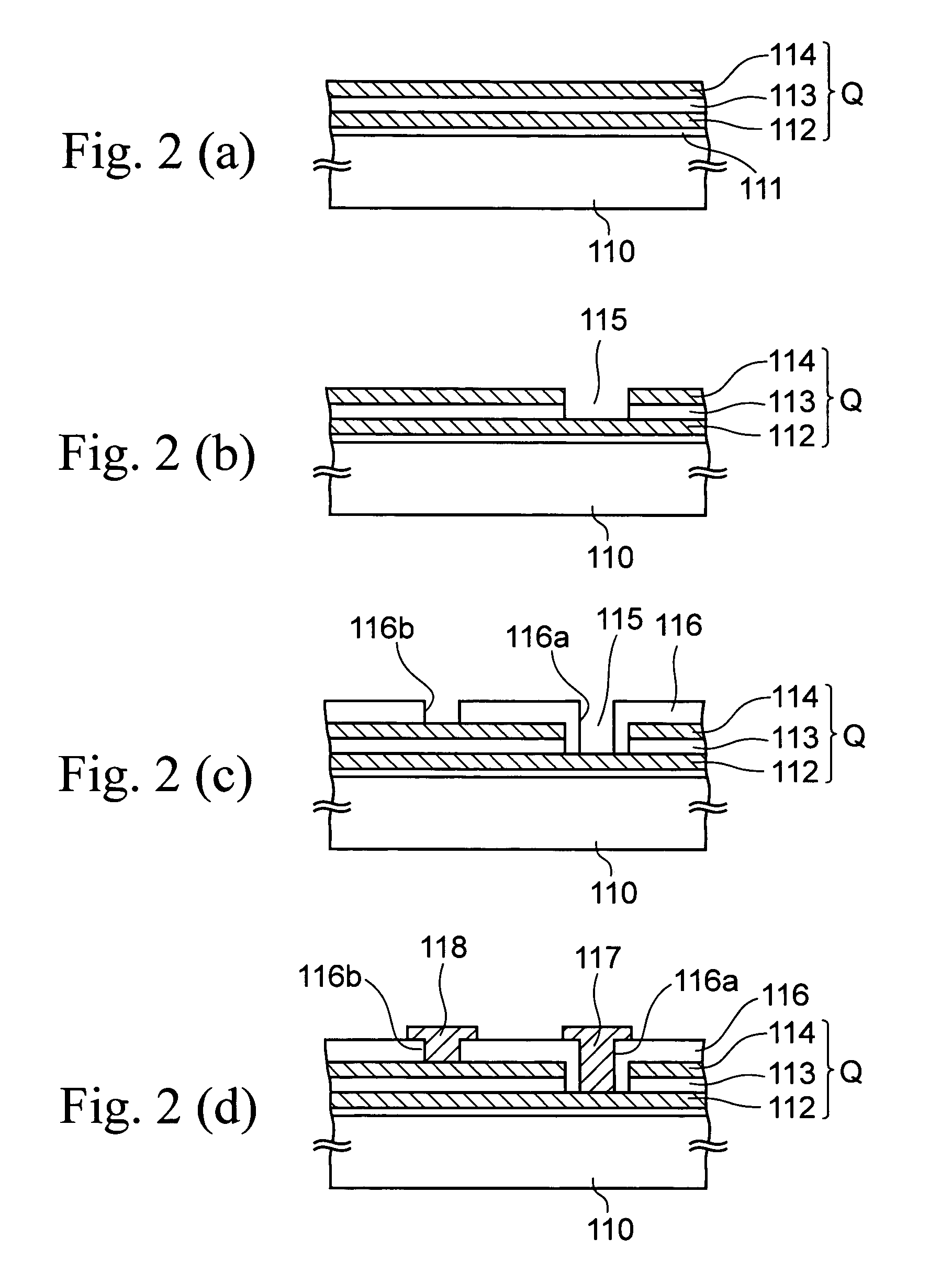
[0062] FIGS. 4 to 7 are cross-sectional views of a capacitive element in the process of being manufactured according to a first embodiment of the present invention.

[0063] In order to manufacture this capacitive element, first, as shown in FIG. 4(a), a titanium (Ti) layer having a thickness of 300 nm and a copper layer having a thickness of approximately 250 nm are formed on a silicon substrate (supporting substrate) 10 as an adhesion layer 11 by sputtering.

[0064] Next, for this substrate 10, liquid polyimide resin (varnish) dissolved in a solvent is applied on the adhesion layer 11 by spin-coating under the following conditions: the number of revolutions is 1000 rpm, and the coating time is 30 seconds. Subsequently, this substrate 10 is put on a hot plate (not shown), and this polyimide resin is precured by heating at a substrate temperature of 90° C., and is then thermoset by baking at a substrate temperature of 400° C., thus forming a base 12 in a film form h...

second embodiment

(2) SECOND EMBODIMENT

[0100] This embodiment differs from the first embodiment only in materials constituting the lower barrier layer 13 and the upper barrier layer 20, but is the same as the first embodiment in the other aspects. Accordingly, a description will be given with reference to FIGS. 4 to 7 of the first embodiment.

[0101] In the first embodiment, the upper barrier layer 20 is made of the alumina layer. On the other hand, in this embodiment, the barrier layer 20 is made of the same material as the capacitor dielectric layers 15a, e.g., BST or PZT, in the step of FIG. 6(b).

[0102] For example, in the case where the capacitor dielectric layers 15a are made of BST, the BST is deposited on the capacitors Q1 and Q2 to a thickness of 100 nm by sputtering using a gas mixture of Ar gas and O2 gas as sputtering gas. The deposited BST is used as the upper barrier layer 20. As deposition conditions in this case, for example, the following conditions are employed: the Ar gas to O2 gas ...

third embodiment

(3) THIRD EMBODIMENT

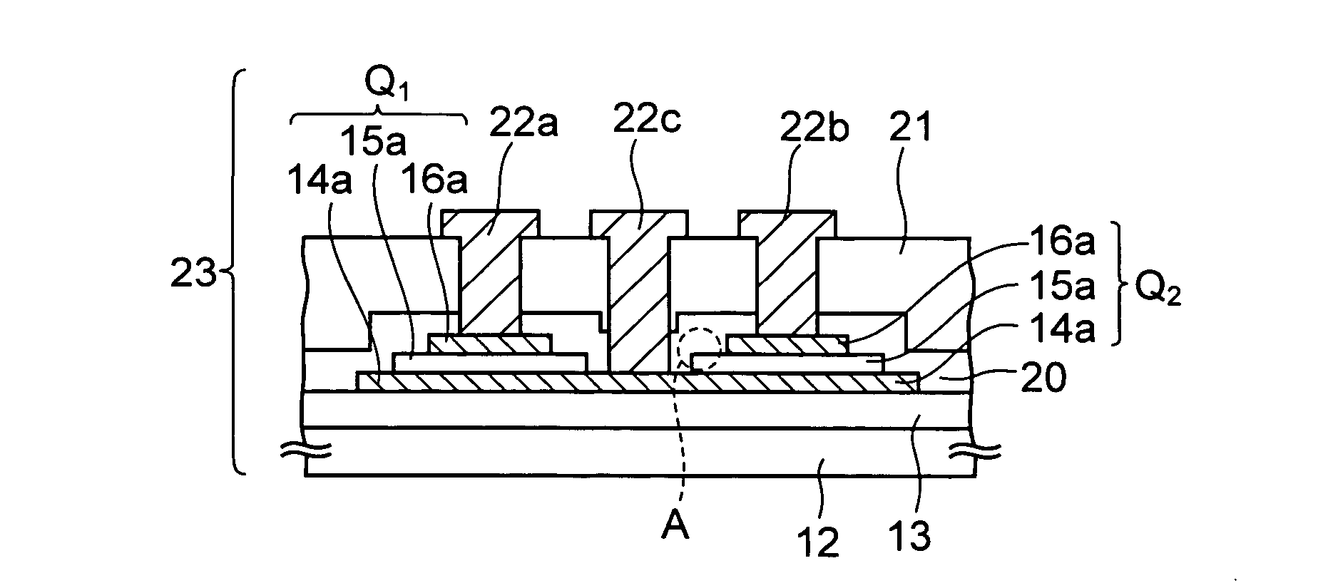
[0105]FIG. 9 is a cross-sectional view of a semiconductor device according to this embodiment.

[0106] As shown in FIG. 9, this semiconductor device is made by mounting the capacitive element 23 fabricated in the first or second embodiment on a semiconductor element 32 such as an LSI. First electrode pads 33a to 33c are provided in the semiconductor element 32, and the first electrode pads 33a to 33c correspond to the respective pads 22a to 22c of the capacitive element 23. The electrode pads 33a to 33c are made of Au, and electrically and mechanically connected to the pads 22a to 22c by ultrasonic bonding.

[0107] The function of the capacitive element 23 in this case is not particularly limited, but the capacitive element 23 is preferably used as decoupling capacitors for the semiconductor element 32.

[0108] Furthermore, second electrode pads 34 are provided in the semiconductor element 32, and the second electrode pads 34 are electrically and mechanically connec...


PUM

PropertyMeasurementUnit
total heightaaaaaaaaaa
thicknessaaaaaaaaaa
thicknessaaaaaaaaaa

Abstract

A capacitive element is characterized by including: a base (12); a lower barrier layer (13) formed on the base (12); capacitors (Q1 and Q2) made by forming a lower electrode (14a), capacitor dielectric layers (15a), and upper electrodes (16a) in this order on the lower barrier layer (13); and an upper barrier layer (20) covering at least the capacitor dielectric layers (15a) and the lower barrier layer (13).

Description

CROSS-REFERENCE TO RELATED APPLICATIONS [0001] This application is a continuation of prior International Patent Application No. PCT / JP2004 / 10132, filed Jul. 15, 2004, the entire contents of which are incorporated herein by reference. TECHNICAL FIELD [0002] The present invention relates to a capacitive element, a method of manufacture of the same, and a semiconductor device. BACKGROUND ART [0003] LSIs such as microprocessors are used by being mounted on circuit boards. It is rare that only an LSI is mounted on a circuit board. Usually, a decoupling capacitor is also mounted on the circuit board. The decoupling capacitor plays roles of reducing fluctuations in supply voltage line in a case of sudden fluctuations in the load impedance of the LSI or the like, and of reducing switching noise to stabilize the operation of the LSI in a high-frequency region of GHz. The performance of the decoupling capacitor needs to be improved in order to further enhance the speed of a semiconductor devi...

Claims


Application Information

Patent Timeline
Patent Type & Authority Applications(United States)
IPC IPC(8): H01L29/00H01G4/33H01G4/40H01L23/12
CPCH01G4/33Y10T29/435H01L28/55H01L28/65H01L28/75H01L2224/45144H01L27/0805H01L2924/30107H01L2924/3011Y10S438/957Y10S257/924H01L2924/19104H01L2924/19103H01L2924/15311H01L2924/1515H01L2224/73265H01L2224/16225H01L2224/32245H01L2224/48247H01L2924/00012H01L2924/00H01L2924/12044H01L24/73H01L2924/181H01L2224/16265
Inventor SHIOGA, TAKESHIBANIECKI, JOHN DAVIDKURIHARA, KAZUAKI
Owner FUJITSU LTD
Why Eureka
Try Eureka