Power semiconductor packaging method and structure

Active Publication Date: 2007-02-22
GENERAL ELECTRIC CO
View PDF17 Cites 61 Cited by
  • Summary
  • Abstract
  • Description
  • Claims
  • Application Information

AI Technical Summary

Benefits of technology

[0008] The present application is directed to various power semiconductor packaging structures and methods of making the packaging structures. The various disclosed embodiments may have one or more of the following benefits: removal of organic adhesive material and/or other organic materials that may limit device operation or cause undesirable stresses at certain elevated temperatures, during applications involving wide thermal cycles or in high moisture environments; employi

Problems solved by technology

However, operating wide band gap power devices at high temperatures puts severe limitations on the packaging, assembly, interconnection materials, processes and structures.
Packaging structures incorporating these technologies generally cannot be subjected to continuous exposure of relatively high temperatures without facing issues of degradation and reliability.
For applications involving very cold temperatures or wide thermal cycles, the use of these organic adhesion layers may cause undesirable levels of thermal stress on packaging structures.
Using polymers in packaging structures which are not hermetically sealed may also cause problems in high moisture environments, since polymers tend to absorb moisture.
Absorption of moisture can have undesirable effects, including raising the dielectric constants of the polymers and increasing parasitic capacitances.
Packaging approaches that do not contain organic polymer materials are generally complex, costly and have poor electrical performance.
However, incorporating interconnect structures on ceram

Method used


Image

  • Power semiconductor packaging method and structure
  • Power semiconductor packaging method and structure
  • Power semiconductor packaging method and structure

Examples


Embodiment Construction

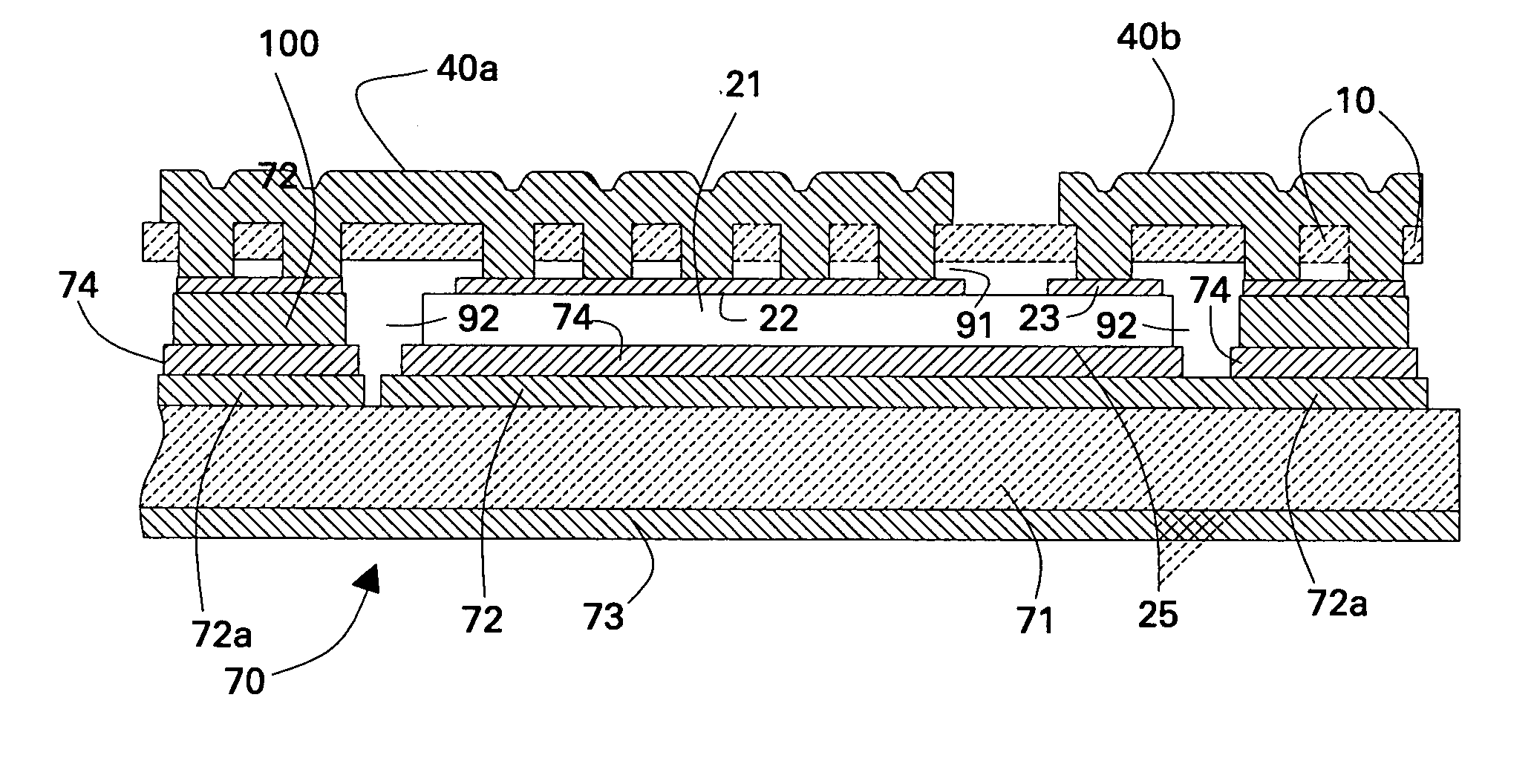
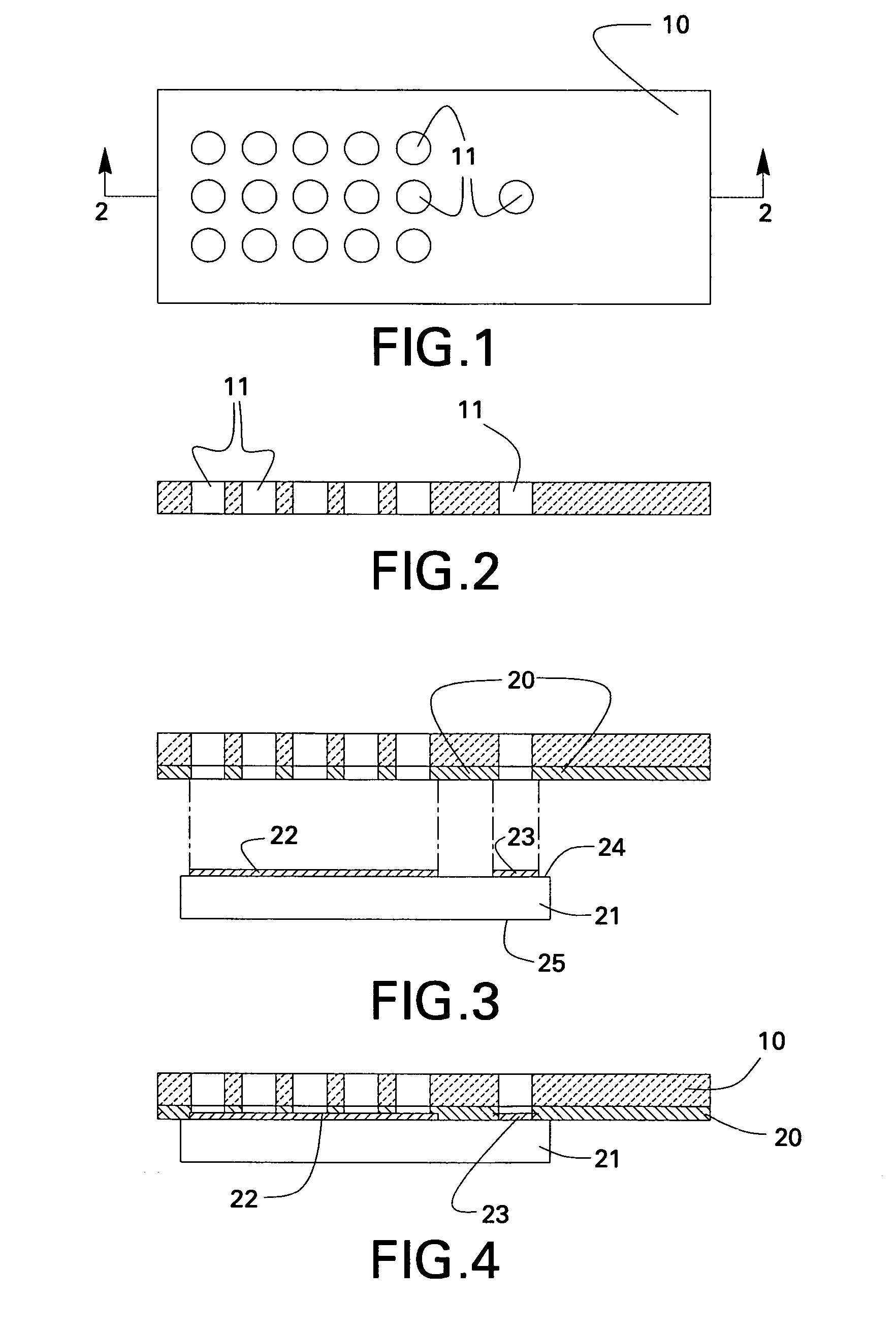
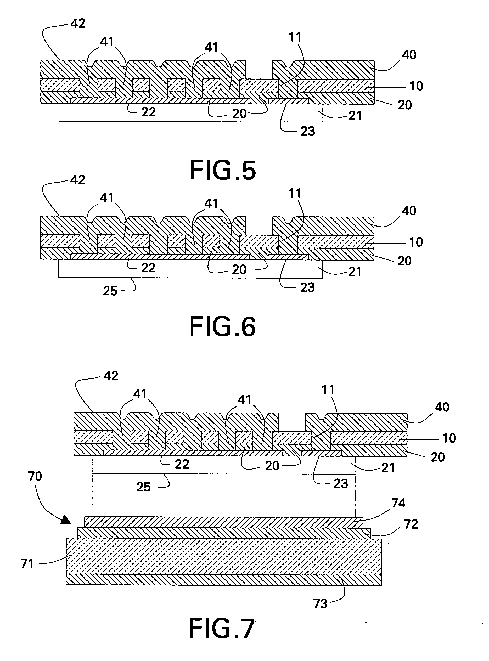
[0031] In the following description, reference is made to the accompanying drawings, which show by way of illustration specific exemplary embodiments in which the invention may be practiced. These embodiments are described in sufficient detail to enable those skilled in the art to practice the invention, and it is to be understood that other embodiments may be utilized and that changes may be made without departing from the scope of the present invention. The following description is, therefore, not to be taken in a limited sense. Wherever possible, the same reference numbers are used throughout the drawings to refer to the same or like parts.

[0032] The temperature at which any given semiconductor packaging structure may continuously be used depends upon, among other things, the materials employed in the packaging structure and the ability of the structure for withstanding thermal stress. Generally speaking, inorganic materials can usually withstand higher temperatures than organic...


PUM


Abstract

A semiconductor chip packaging structure comprising a dielectric film having one or more through holes aligned with the one or more contact pads of at least one power semiconductor chip. A patterned electrically conductive layer adjacent to the dielectric film has one or more electrically conductive posts which extend through the one or more though holes aligned with the contact pads to electrically couple the conductive layer to the contact pads. In certain embodiments, one or more air gaps may be formed between the dielectric film and the active surface of the at least one power semiconductor chip. Methods for fabricating the semiconductor chip packaging structure are also disclosed.

Description

BACKGROUND OF THE INVENTION [0001] The present application relates generally to structures and methods for packaging power semiconductor devices. [0002] Wide band gap semiconductor devices, such as SiC devices, have the ability to operate at highly elevated temperatures for some power electronics applications, without degrading device performance or developing failure mechanisms that would limit operating life. This attribute has the potential benefit of permitting high power operation in high temperature environments without expensive cooling structures and materials that would be required if lower operating temperatures had to be maintained. However, operating wide band gap power devices at high temperatures puts severe limitations on the packaging, assembly, interconnection materials, processes and structures. [0003] In the past, semiconductor packaging technologies were designed for the known temperature limits of silicon and gallium arsenide devices, which are near the 125° C. ...

Claims


Application Information

Patent Timeline
IPC IPC(8): H01L31/111H01L21/48
CPCH01L2924/10329H01L2924/13055H01L2924/13091H01L2924/19042H01L2924/30105H01L2924/30107H01L23/4821H01L23/4822H01L23/5385H01L23/5389H01L24/24H01L24/82H01L25/072H01L2224/2402H01L2224/24226H01L2224/82039H01L2224/82047H01L2224/92135H01L2924/01005H01L2924/01013H01L2924/01015H01L2924/01027H01L2924/01029H01L2924/01032H01L2924/01033H01L2924/01042H01L2924/01046H01L2924/01049H01L2924/01074H01L2924/01078H01L2924/01079H01L2924/01082H01L2924/09701H01L2924/01006H01L2924/01019H01L2924/01023H01L2924/01047H01L2924/01076H01L2924/014H01L2224/92144H01L2224/73267H01L2224/32225H01L2924/00H01L2224/24137H01L2924/351H01L2924/1306H01L2924/15787H01L2924/1305H01L2924/12042H01L2224/0603
Inventor FILLION, RAYMOND ALBERTBEAUPRE, RICHARD ALFREDELASSER, AHMEDWOJNAROWSKI, ROBERT JOHNKORMAN, CHARLES STEVEN
Owner GENERAL ELECTRIC CO
Why Eureka
Try Eureka