

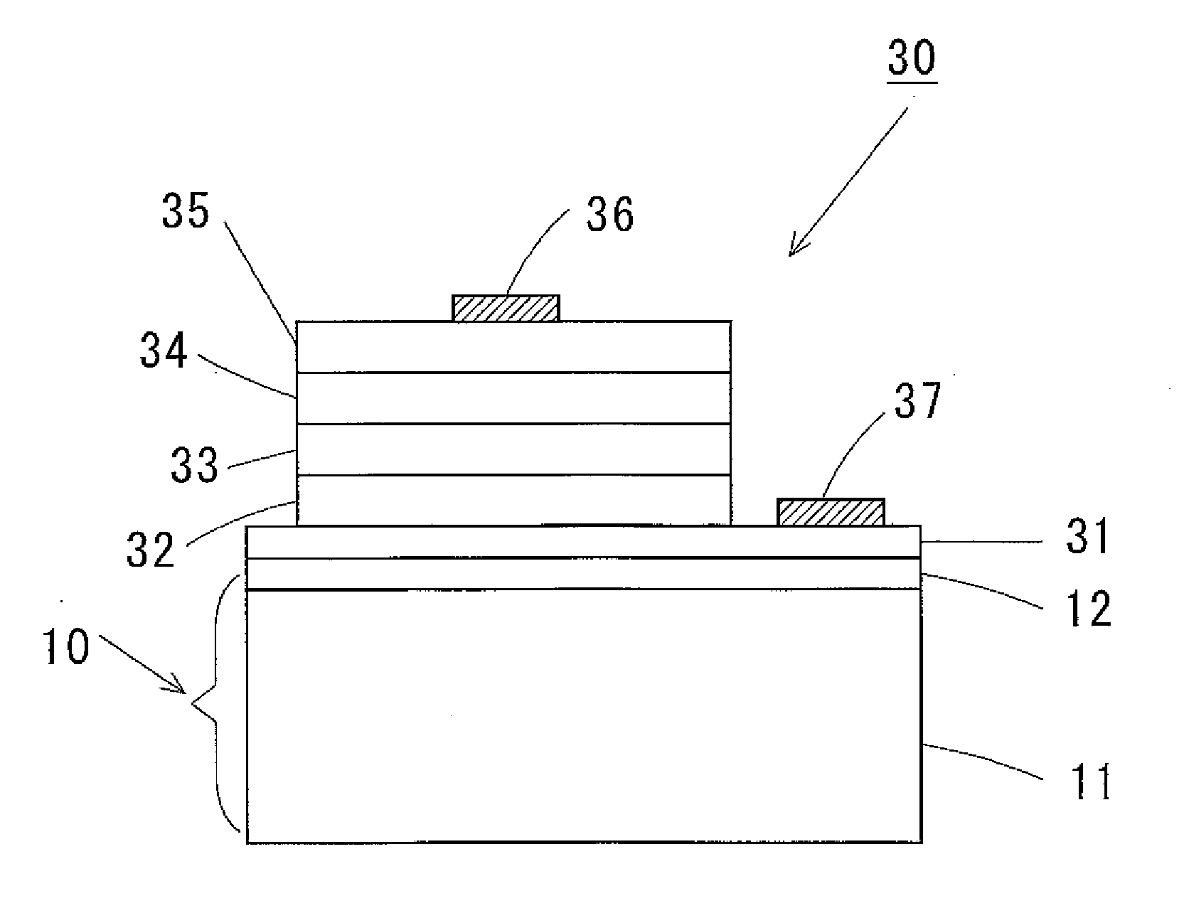
Substrate for film growth of group iii nitrides, method of manufacturing the same, and semiconductor device using the same
a technology of nitride and substrate, which is applied in the direction of semiconductor/solid-state device manufacturing, semiconductor devices, electrical devices, etc., can solve the problems of high manufacturing cost of substrate with buffer layer attached thereon, difficult formation of thin films, and cloudiness in grown aln thin films. , to achieve the effect of reducing cracks and pits, reducing the occurrence of cracks and pits, and more stabilization
- Summary
- Abstract
- Description
- Claims
- Application Information
AI Technical Summary
Benefits of technology
Problems solved by technology
Method used
Image

Examples
example 1
[0077] Hereinafter, the present invention is explained in more detail referring to the examples.
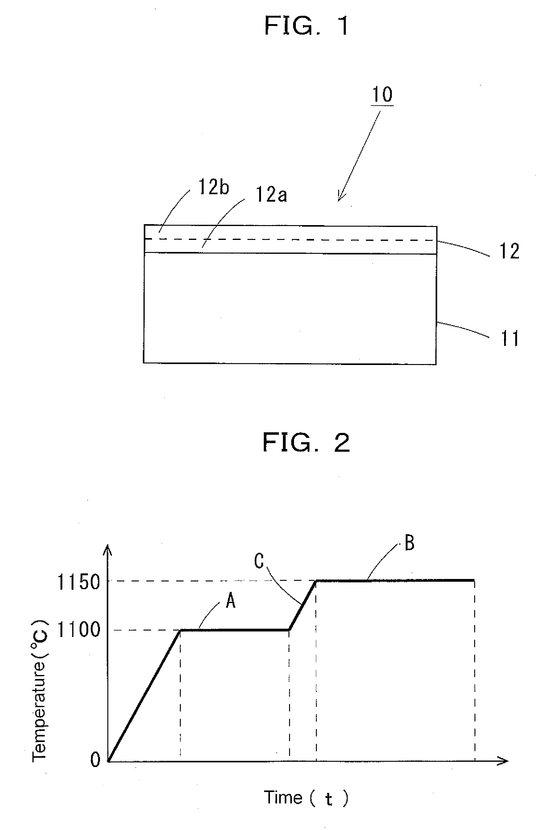
[0078] The method of manufacturing the substrate material 11 for film growth of group III nitride of the present invention will be explained first.
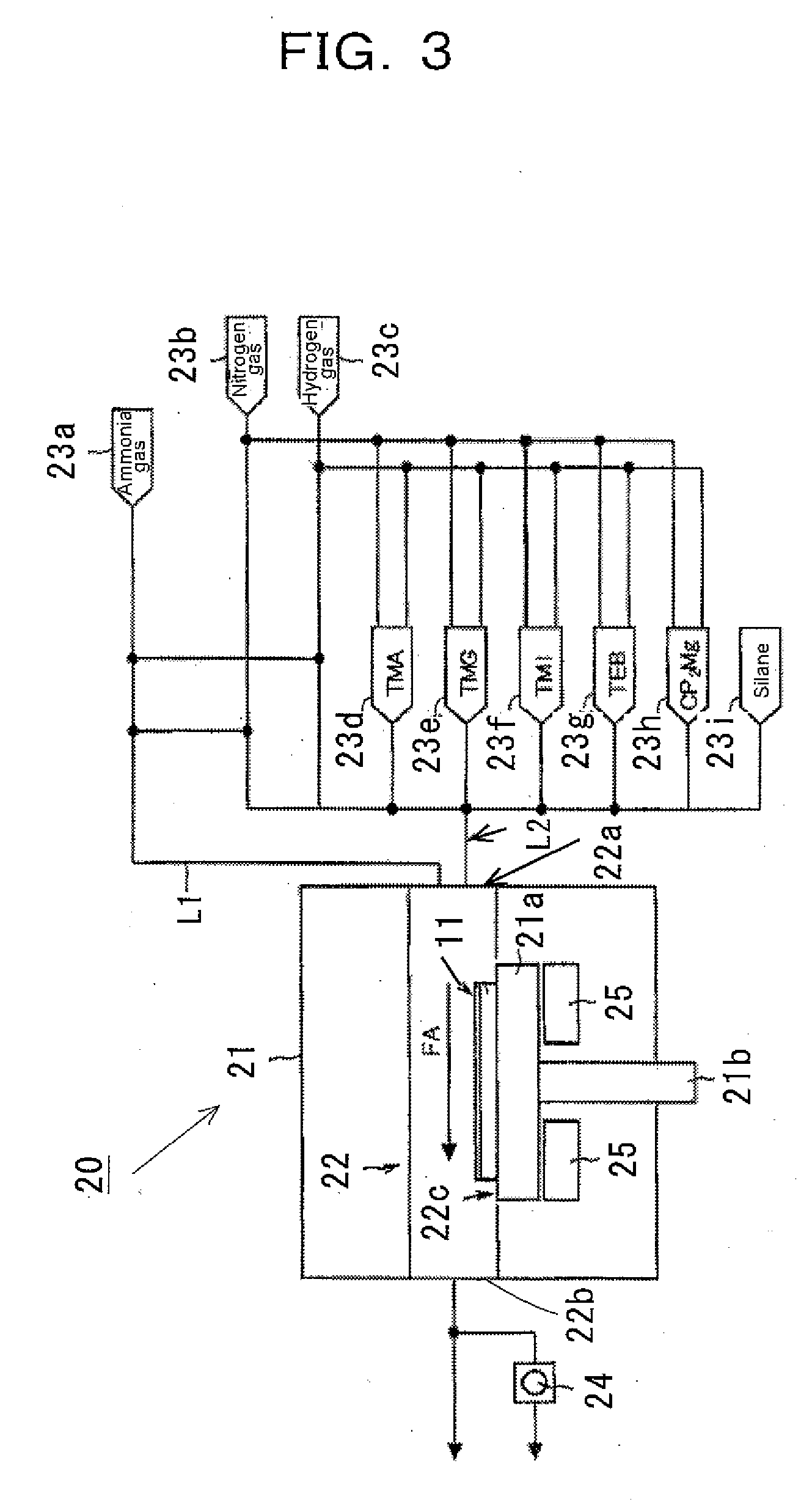
[0079] As a substrate material 11, a (0001) plane sapphire single crystal of 2 inch diameter and 400 μm thickness. Table 1 is a table showing each film growth condition in Examples 1-4 of manufacturing the substrate for film growth of group III nitride by using the manufacturing apparatus of FIG. 3.
[Table 1]
[0080] In each Example, after setting the pressure in the reactor vessel 21 of the manufacturing apparatus 20 to 15 Torr, the hydrogen gas was flown as the carrier gas at 350 milli mole (mmole) / minute, and the substrate material 11 was treated for cleaning by heating at a pre-determined temperature, and next the surface of the substrate material 11 was treated for making nitride by supplying ammonia gas. After that, a first layer AlN thi...
example 2
[0085] Example 2 will be explained next.
[0086] In Example 2, after treating for cleaning with hydrogen gas at 1100° C. for 10 minutes and treating for making nitride at 1100° C. for 10 seconds, the growing parameters are set to constant as the pressure of 10 Torr, the film growth temperature 1100° C., and carrier gas feed amount 350 (mmole / minute). As the first step, the film thickness of 0.3 μm was grown with the parameters as the group III source amount 35 (μmole / minute), the group V source amount 4.5 (mmole / minute), and V / III ratio (source gas flow rate ratio) 130. As the second step, the film thickness of 0.3 μm was grown to form the AlN thin film 12 with the parameters as the group III source amount changed as 35, 17.5, 52.5, 35, and 35 (μ mole / minute), accompanied by the change of group V source amount as 4.5,4.5,4.5,9.0, and 1.8 (mmole / minute), and the change of V / III ratio (source gas flow rate ratio) as 130, 260, 86, 260 and 50 (to be called Examples 2-1 to 2-5, respective...
example 3
[0088] Example 3 will be explained next.
[0089] In Example 3, after cleaning with hydrogen gas at 1100° C. for 10 minutes and treating for making nitride at 1100° C. for 7 minutes, the growth parameters are set to constant as the film growth temperature 1100° C., the group III source amount 40 (μmole / minute), the group V source amount 20 (mmole / minute), V / III ratio (source gas flow rate ratio) 500, and carrier gas feed amount 350 (mmole / minute). As the first step the AlN thin film 12 of film thickness 0.3 μm was formed at pressure 15 Torr, and at a second step the film thickness of 0.3 μm was grown to form the AlN thin film as the pressures changed to 8, 10, 15, and 20 Torr (to be called Examples 3-1 to 3-5, respectively).
[0090]FIG. 11 is a graph showing the pit density of the AlN thin film surface formed on the substrate for film growth of group III nitride in Example 3. As is shown in FIG. 11, the pit density ( / cm2) of the AlN thin film surface is confirmed to be improved to 2×10...
PUM
| Property | Measurement | Unit |
|---|---|---|
| thickness | aaaaa | aaaaa |
| temperature | aaaaa | aaaaa |
| thickness | aaaaa | aaaaa |
Abstract
Description
Claims
Application Information