Method for forming memory cell and periphery circuits

a technology of memory cells and periphery circuits, applied in the direction of semiconductor devices, basic electric elements, electrical equipment, etc., can solve the problems of reducing developing minimized devices, etc., and achieve the effect of improving the length of the bird's beak and minimizing devices

Inactive Publication Date: 2007-03-01
MACRONIX INT CO LTD
View PDF9 Cites 12 Cited by
  • Summary
  • Abstract
  • Description
  • Claims
  • Application Information

AI Technical Summary

Benefits of technology

[0017] An object of the present invention is to provide a method for forming memory cell capable of improving

Problems solved by technology

However, the above-mentioned manufacturing process has the following disadvantage.
Therefore, it is impossible to further shrink

Method used


Image

  • Method for forming memory cell and periphery circuits
  • Method for forming memory cell and periphery circuits
  • Method for forming memory cell and periphery circuits

Examples


Embodiment Construction

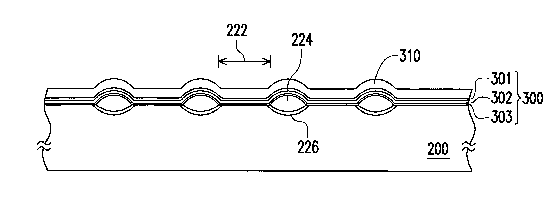
[0029]FIG. 2A-2C are schematic cross-sectional views of a manufacturing process for forming memory cells according to an embodiment of the present invention.

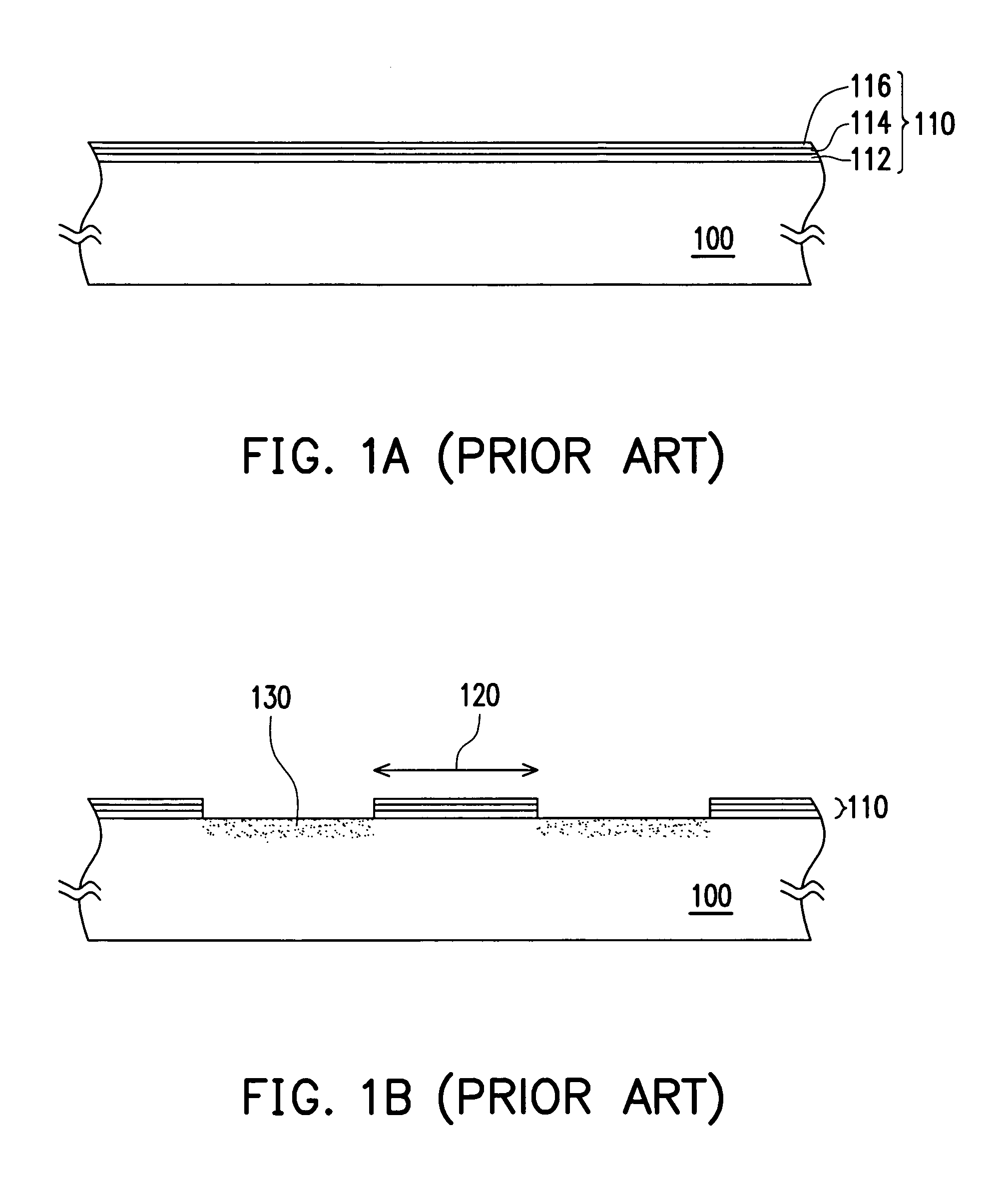
[0030] First, referring to FIG. 2A, a substrate 200 is provided, then a liner layer 210 can be formed on the substrate 200, for example, the liner layer 210 is pad oxide layer. Next, a mask layer 220 is formed on the liner layer 210 in order to define a plurality of tunnel regions 222 on the substrate 200; for example, a material of the mask layer 220 is dielectric such as silicon nitride. Furthermore, a plurality of dopants 212, such as boron or arsenic, is implanted in the substrate 200 between the tunnel regions 222. After implanting the dopants 212, a tilt ion implant process can be optionally performed for pocket implant (not shown).

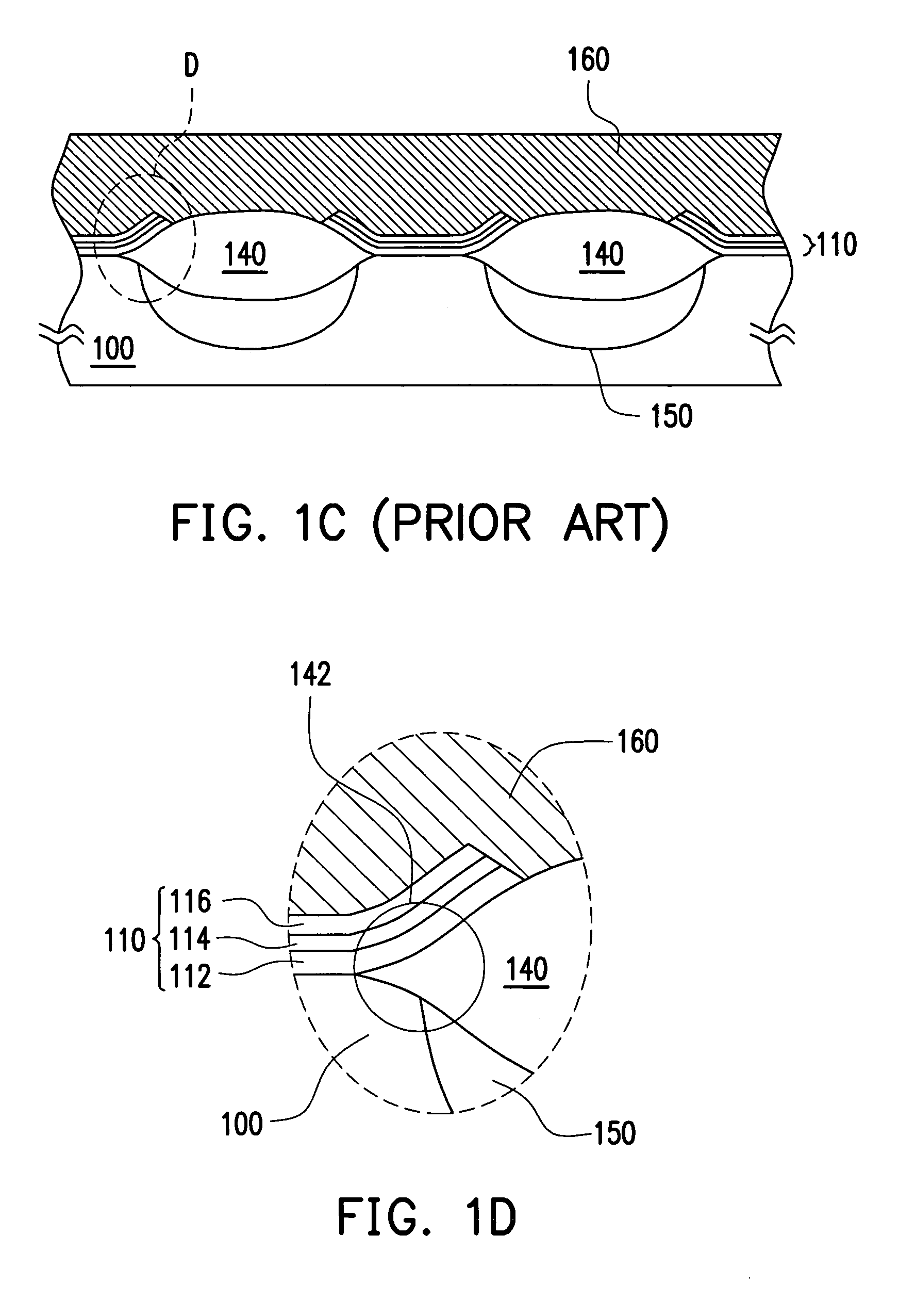
[0031] Further, as shown in FIG. 2B, using the liner layer 210 and the mask layer 220 as masks, a plurality of inter-cell isolation layers 224 is formed on the substrate 200 between the channe...


PUM


Abstract

A method for forming a memory cell and periphery circuit includes providing a substrate with a peripheral circuit region and a memory cell region. A mask layer is formed on the substrate to define multiple active regions in the peripheral circuit region and to define multiple channel regions in the memory cell region. Multiple field oxide layers are formed between the active areas, and Dopants are implanted in the substrate between the channel regions. Multiple inter-cell isolation layers are formed between the channel regions and the dopants are driven in the substrate to form buried diffusion regions. The mask layer is removed. A layer of electricity-storage material and multiple word lines are formed on the substrate in the memory cell region.

Description

BACKGROUND OF THE INVENTION [0001] 1. Field of the Invention [0002] This invention generally relates to a method for forming a transistor device, and especially to a method for forming memory cells and simultaneously forming memory cells and periphery circuits. [0003] 2. Description of Related Art [0004] The memory, which is used for storing electronic data, is one of the important components in the semiconductor. In genera, the memory that can store electronic data without periphery power supply is called the Non-Volatile Memory device. [0005] The current non-volatile memory comprises an erasable programmable ROMs (EPROMs), electrically erasable programmable ROMs (EEPROMS) and Flash memory. These memories can be operated by channel hot electron (CHE) injecting or fowler-nordheim (F-N) tunneling field emission mechanism. [0006] Take the flash memory as an example, which comprises a stack-type gate structure on a semiconductor substrate, wherein the stack-type gate structure comprise...

Claims


Application Information

Patent Timeline
IPC IPC(8): H01L21/336
CPCH01L27/11568H01L27/115H10B69/00H10B43/30
Inventor KIM, JONGOHLIU, CHENG-JYE
Owner MACRONIX INT CO LTD
Why Eureka
Try Eureka