Optical semiconductor device

Inactive Publication Date: 2007-03-08
OCLARO JAPAN INC
View PDF1 Cites 25 Cited by
  • Summary
  • Abstract
  • Description
  • Claims
  • Application Information

AI Technical Summary

Benefits of technology

[0017] In the present invention, the strain-compensated type of MQW structure constructed of the InGaAlAs-strained quantum well layers and the InGaAlAsSb-strained barrier layers allows ΔEc and ΔEv to be arbitrarily set. This structure is therefore effective in achieving device resistance reduction and differential gain improvement at the same time for the semic

Problems solved by technology

Consequently, the influence of valence band mixing diminishes and effective mass decreases.
In the conduction band, a carrier overflow of electrons occurs, and in the valence band, holes are liable to exist unevenly within the MQW structure.
As a result, overall laser characteristics inclusive of a differential gain will not improve.
For these reasons, with the conventional technology, because of ΔEc and ΔEv being independently uncontrollable, it has been very difficult to obtain a device that simultaneously achieves the improvement of a differential gain and the improvement of laser characte

Method used


Image

  • Optical semiconductor device
  • Optical semiconductor device
  • Optical semiconductor device

Examples


Example

First Embodiment

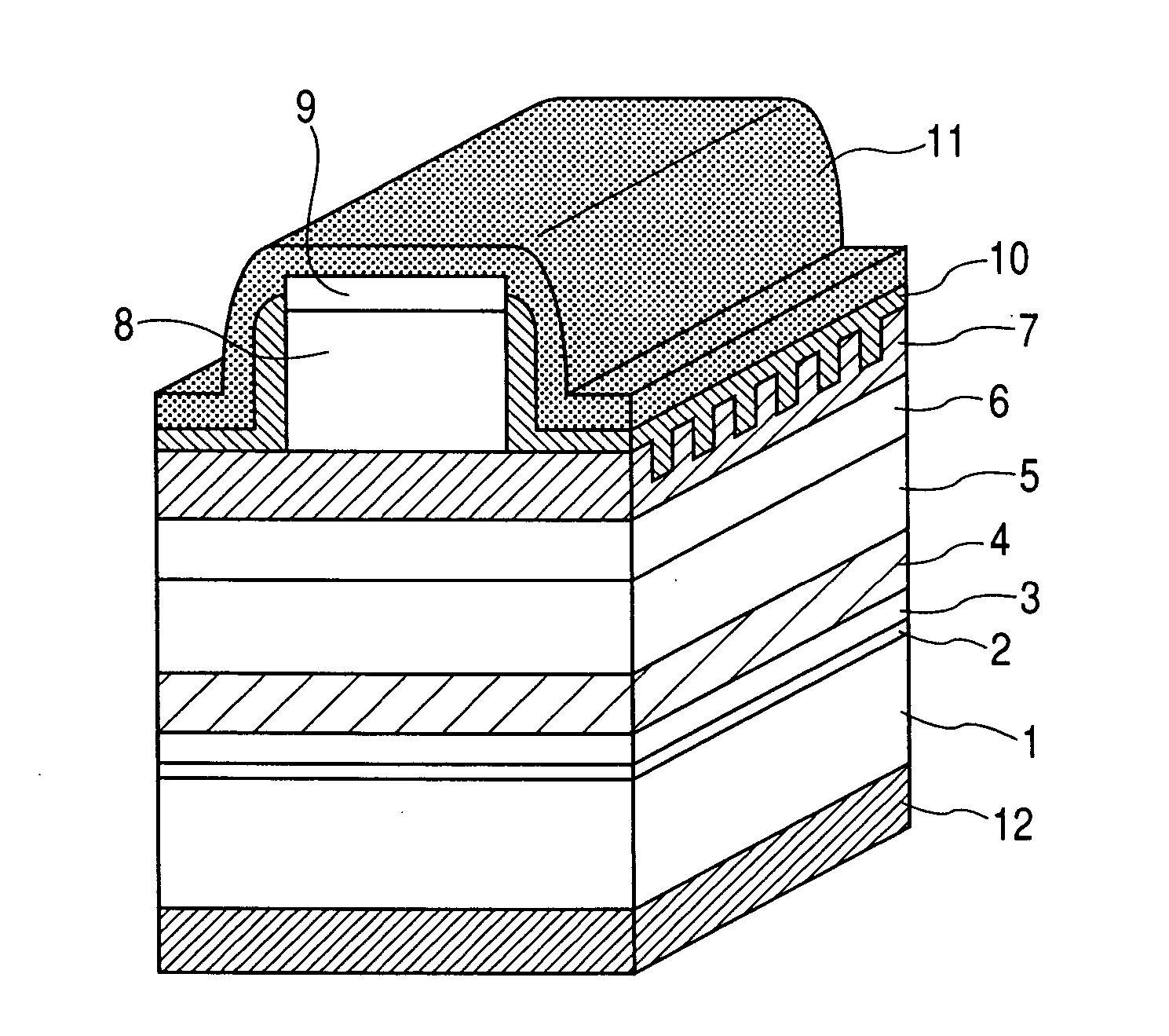
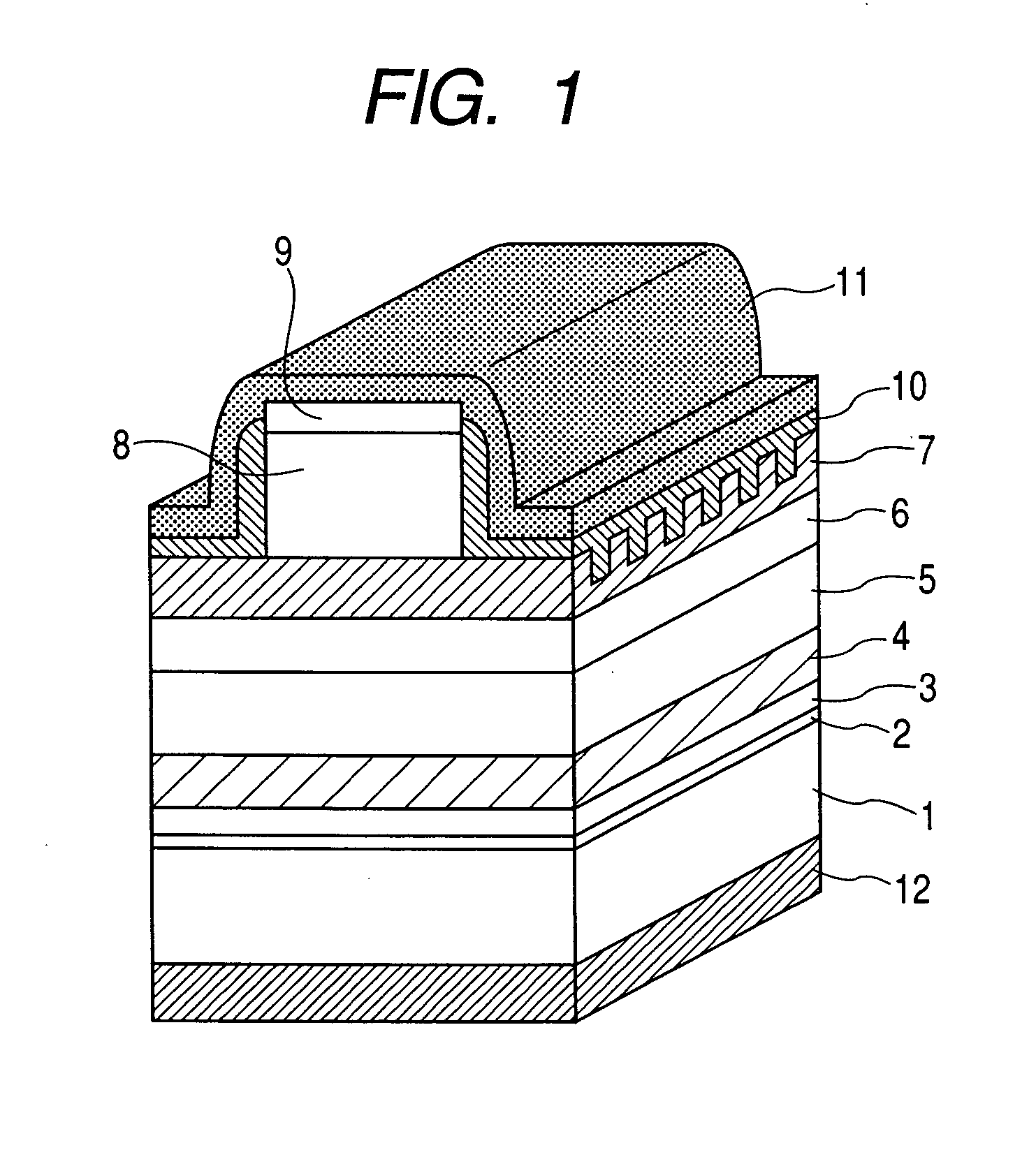
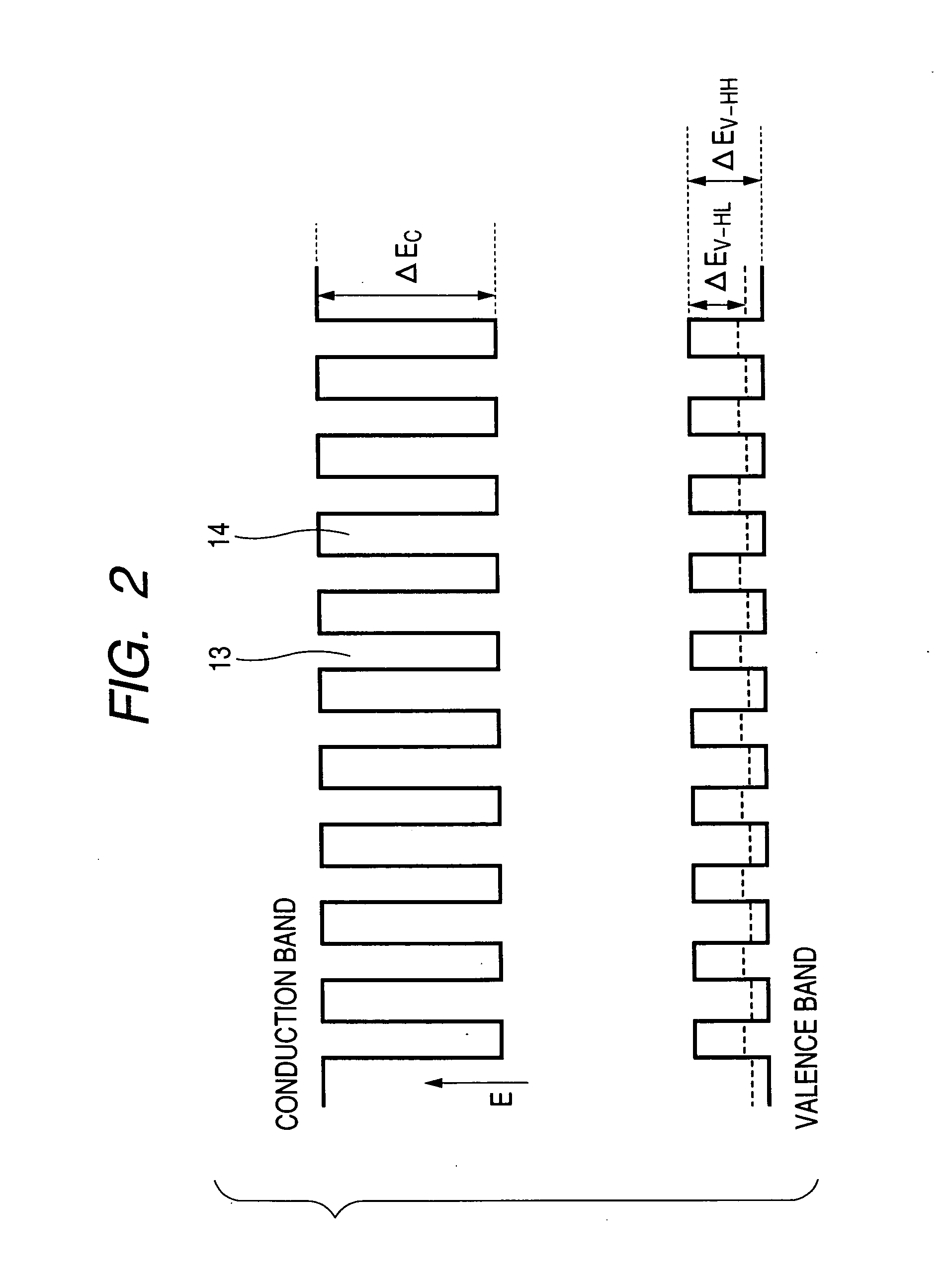
[0032] A first embodiment is an example in which the present invention is applied to a 1.3-μm-band DFB (distributed feedback) laser for optical-fiber communication. This laser can be of a known structure, except for active layers. A perspective view of the laser structure employed in the present embodiment is shown in FIG. 1. Reference number 1 in FIG. 1 denotes an n-type InP wafer, which also functions as a lower cladding layer. Reference number 2 denotes a 30-nm-thick n-type InAlAs layer, and 3 denotes a GRIN-SCH (Graded-Index - Separate Confinement Structure) layer of 0.08-μm-thick n-type InGaAlAs with a carrier concentration of 1×1018 cm−3. Reference number 4 denotes an MQW layer that includes a quantum well layer formed of In0.733Ga0.132Al0.135As, and a barrier layer formed of In0.36Ga0.32Al0.32As0.92Sb0.08. The quantum well layer has a thickness of 5 nm and a compressive strain of 1.4% with respect to the InP wafer, and the barrier layer has a thickness of 8 n...

Example

Second Embodiment

[0040] A second embodiment is an example in which the present invention is applied to a 1.3-μm-band DFB (distributed feedback) laser for optical-fiber communication. This laser can be of a known structure, except for active layers, and a laser of a buried heterostructure, fabricated on such a p-type InP wafer as shown in FIG. 7, is applied in the present embodiment. Reference number 19 in FIG. 7 denotes a p-type InP wafer, which also functions as a lower cladding layer. Reference number 23 denotes an electron-stopping layer of 0.03-μm-thick p-type InAlAs with a carrier concentration of 9×1017 cm−3, and 20 denotes an SCH layer of 0.06-μm-thick p-type InGaAlAs with a carrier concentration of 8×1017 cm−3 and a composition wavelength of 0.92 μm. Reference number 21 denotes an MQW layer that includes a quantum well layer formed of In0.329Ga0.649Al0.022As, and a barrier layer formed of In0.555Ga0.152Al0.293As0.96Sb0.04 (composition wavelength: 1.06 μm) The quantum well l...

Example

Third Embodiment

[0047] A third embodiment is an example in which the present invention is applied to a 1.55-μm-band DFB ridge waveguide laser for communication, fabricated on an InP wafer. Structurally, the present embodiment is essentially equivalent to the first embodiment, except for an MQW layer. The MQW layer includes a quantum well layer formed of In0.734Ga0.0210Al0.056As, and a barrier layer formed of In0.368Ga0.399Al0.233As0.92Sb0.08 (composition wavelength: 984 μm). The quantum well layer is 5 nm thick and has a compressive strain of 1.4% with respect to the InP wafer, and the barrier layer is 8 nm thick and has a tensile strain of −0.5% with respect to the InP wafer. The number of quantum well layers is 12, and the total number of barrier layers arranged at top and bottom of each quantum well layer is 13. Band discontinuity ΔEc of a conduction band in this structure is as great as 409 meV. In a valence band, similarly to the first embodiment, the heavy holes and light hol...


PUM


Abstract

In the semiconductor laser or electro-absorption optical modulator that includes strained quantum well layers as active layers, making laser characteristics or modulator characteristics adequate has seen the respective limits since band structures, especially, ΔEc and ΔEv, have been unable to be adjusted independently.
This invention is constructed by stacking an n-type InGaAlAs-GRIN-SCH layer 3, an MQW layer 4, a p-type InGaAlAs-GRIN-SCH layer 5, a p-type InAlAs electron-stopping layer 6, and others, in that order, on an n-type InP wafer 1; wherein the MQW layer 4 includes InGaAlAs-strained quantum well layers and InGaAlAsSb-formed barrier layers each having strain of an opposite sign to the strain applied to the quantum well layers.

Description

CLAIM OF PRIORITY [0001] The present application claims priority from Japanese application JP 2005-003365, filed on Jan. 11, 2005, the content of which is hereby incorporated by reference into this application. BACKGROUND OF THE INVENTION [0002] 1. Field of the Invention [0003] The present invention relates to optical semiconductor devices, and more particularly, to a communications semiconductor laser, an optical modulator, both for use as an optical-fiber transmission light source, and an electro-absorption light source that is an integrated unit of both. [0004] 2. Description of the Related Art [0005] The proliferation of the Internet on a worldwide scale is increasing the data traffic of optical communications networks each year. In response to this increase, the semiconductor-based transmission light sources and optical modulators that are among the key devices in optical-fiber communications networks, or electro-absorption light sources that are each an integrated unit of the ...

Claims


Application Information

Patent Timeline
IPC IPC(8): H01L31/00H01S5/12
CPCB82Y20/00Y10S438/962G02F2001/01766H01S5/0265H01S5/0287H01S5/12H01S5/1221H01S5/227H01S5/305H01S5/3054H01S5/3406H01S5/34306H01S5/34313H01S5/34366G02F1/01708G02F1/01766
Inventor NAKAHARA, KOUJIKUDO, MAKOTOTANAKA, SHIGEHISASHIRAI, MASATAKA
Owner OCLARO JAPAN INC
Why Eureka
Try Eureka