Photoelectric conversion layer, photoelectric conversion device and imaging device, and method for applying electric field thereto

a technology of photoelectric conversion and imaging device, which is applied in the direction of electrical apparatus, semiconductor/solid-state device manufacturing, and semiconductor devices. it can solve the problems of inevitably large dimension and weight of imaging devices of such a tree-plate type structure, and achieve high photoelectric conversion efficiency, excellent durability, and high resolution

Inactive Publication Date: 2007-03-08
FUJIFILM HLDG CORP +1
View PDF7 Cites 68 Cited by
  • Summary
  • Abstract
  • Description
  • Claims
  • Application Information

AI Technical Summary

Benefits of technology

[0025] The photoelectric conversion layer, the photoelectric conversion device and the imaging device according to the invention have advantages such as high photoelectric conversion efficiency and excellent durability. In two-layer stack type and BGR three-layer stack type solid imaging devices, there are the following characteristic features in addition to the foregoing advantages.
[0026] Because of a stacked structure, a moiré pattern is not generated, resolution is high because an optical low pass filter is not required, and color blur is not formed. Furthermore, a signal treatment is simple, and a pseudo signal is not generated. In addition, in the case of CMOS, mixing of pixels is easy, and partial reading is easy.
[0027] Since an aperture is 100% and a micro lens is not required, there is no limitation in an exit pupil distance against camera lens, and there is no shading. Accordingly, the invention is suitable for lens interchangeable cameras. On this occasion, it becomes possible to make the lens thin.
[0028] Since a micro lens is not required, it becomes possible to seal a glass by filling with an adhesive. Thus, it is possible to make a package thin and increase the yield, resulting in a reduction of costs.
[0029] Since an organic dye is used, high sensitivity is obtained, an IR filter is not required, and a flare is lowered.

Problems solved by technology

However, imaging devices of such a tree-plate type structure inevitably become large in both the dimension and the weight from the standpoint of structure.

Method used


Image

  • Photoelectric conversion layer, photoelectric conversion device and imaging device, and method for applying electric field thereto
  • Photoelectric conversion layer, photoelectric conversion device and imaging device, and method for applying electric field thereto
  • Photoelectric conversion layer, photoelectric conversion device and imaging device, and method for applying electric field thereto

Examples


example 1

[0217] A rinsed ITO substrate was placed in a vapor deposition device and subjected to vapor deposition with the following Compound (A) as an n-type organic semiconductor in a thickness of 50 nm. The following Compound (B) as a p-type organic dye was subsequently subjected to vapor deposition in a thickness of 100 nm thereon, thereby preparing an organic pn stack type photoelectric conversion layer. Next, Compound (1) of the invention as an electron block material was subjected to vapor deposition in a thickness of 50 nm. Next, a patterned mask (with a light receiving area of 2 mm×2 mm) was placed on the organic thin layer and subjected to vapor deposition with aluminum in a thickness of 100 nm within the vapor deposition device, and a drying agent was subsequently charged, thereby sealing the device. There was thus prepared a photoelectric conversion device (Device 1).

example 2

[0218] A device (Device 2) was prepared ill exactly the same manner as in Example 1, except for using Compound (2) of the invention in place of the Compound (1) of the invention.

example 3

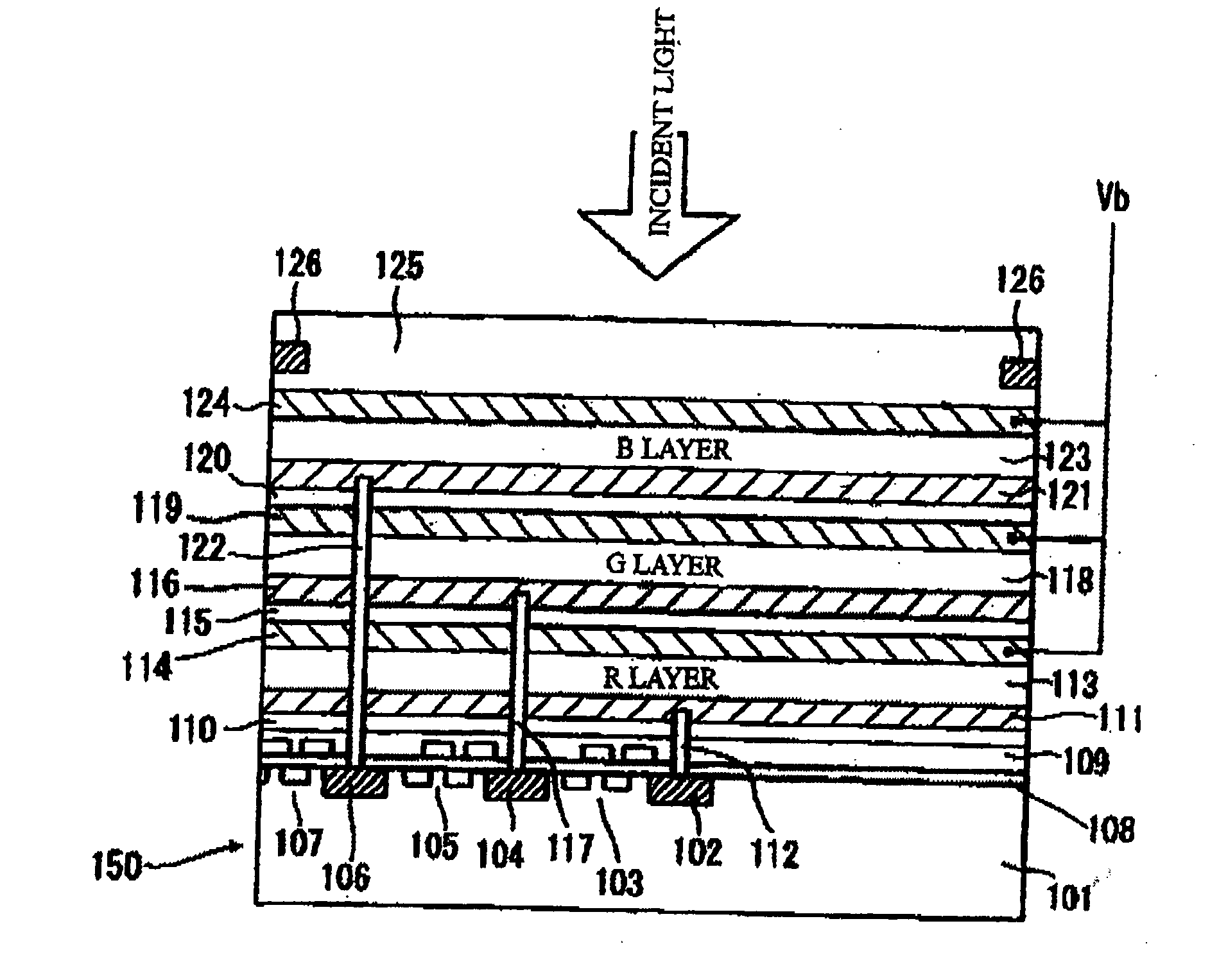
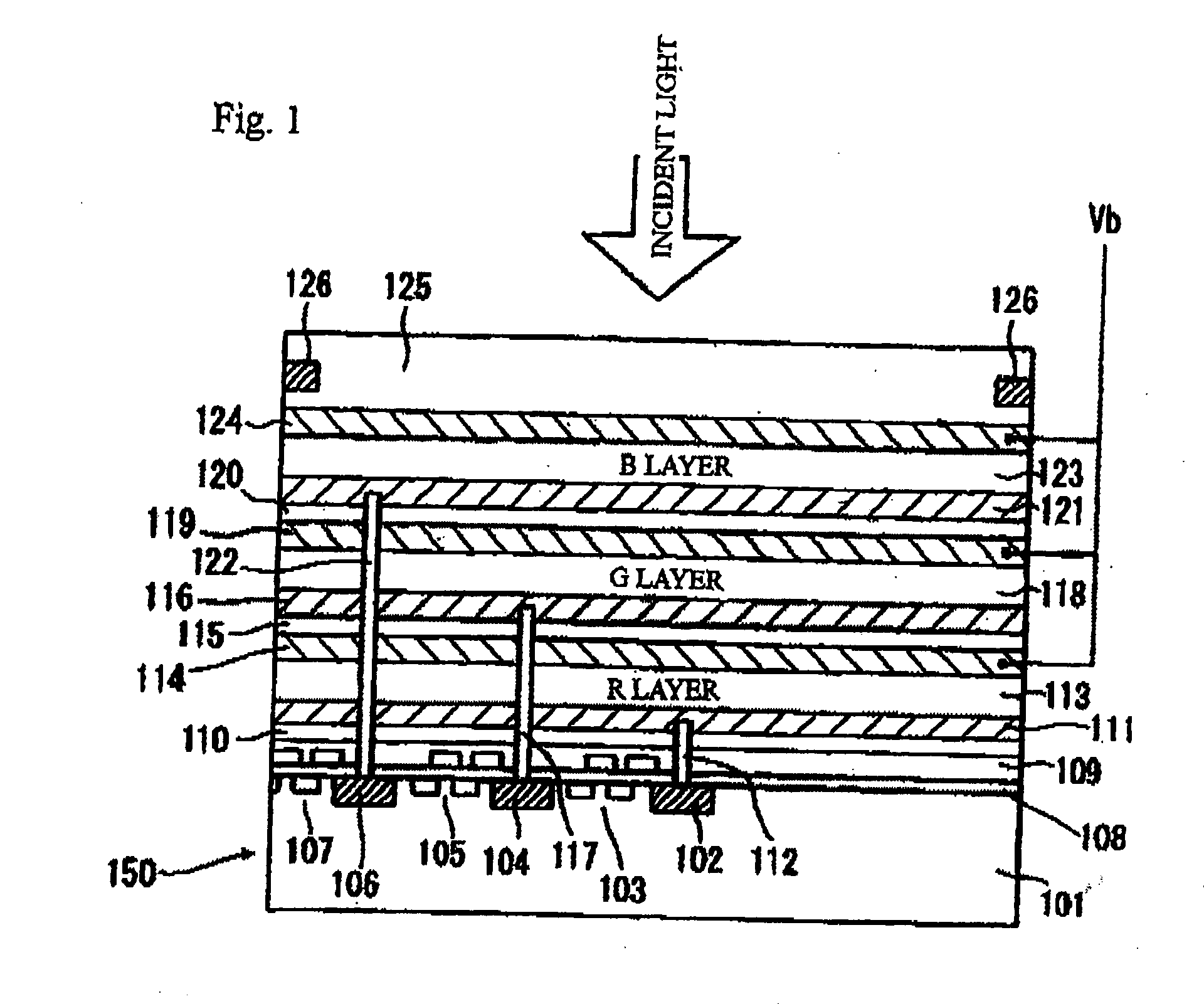
[0224] By using the device of Example 1 according to the invention in the G layer as shown in FIG. 1, it is possible to prepare a color imaging device exhibiting excellent color separation.

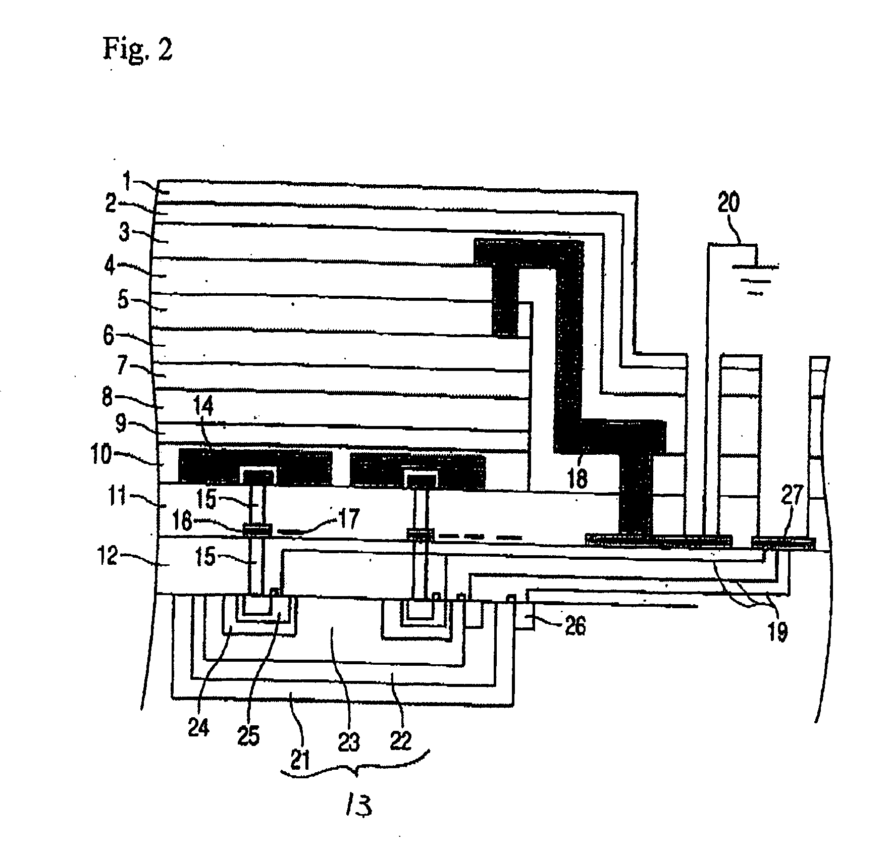
[0225] By using the photoelectric conversion site of Example 1 or 2 which is capable of absorbing G light in the portions 8 and 9 of the photoelectric conversion site as shown in FIG. 2, it is possible to prepare a color imaging device exhibiting excellent color separation.


PUM


Abstract

A photoelectric conversion layer comprising a compound represented by the following formula (1):
wherein R1 to R10 each independently represents a hydrogen atom or a substituent; L represents a monovalent group or a divalent or polyvalent connecting group; m is 0 or 1; and n represents an integer of from 1 to 4.

Description

FIELD OF THE INVENTION [0001] The present invention relates to a photoelectric conversion layer, a photoelectric conversion device having the photoelectric conversion layer and a solid imaging device, and to a method for applying an electric field thereto and an applied device. BACKGROUND OF THE INVENTION [0002] A photoelectric conversion layer is widely utilized in, for example, optical sensors and in particular, is suitably used as a solid imaging device (light receiving device) of imaging device (solid imaging device) such as a television camera. As materials of the photoelectric conversion layer which is used as the solid imaging device of imaging device, layers made of an inorganic material such as Si layers and a-Se layers are mainly used. [0003] Conventional photoelectric conversion layers using such an inorganic material layer do not have sharp wavelength dependency against photoelectric conversion layer characteristics. For that reason, as to an imaging device using a photo...

Claims


Application Information

Patent Timeline
Patent Type & Authority Applications(United States)
IPC IPC(8): H01L31/00
CPCH01L31/101H01L27/14647
Inventor OSAKA, ITARUHAYASHI, MASAYUKI
Owner FUJIFILM HLDG CORP
Why Eureka
Try Eureka